JAJSE28B October 2017 – August 2018 UCC27710
PRODUCTION DATA.
- 1 特長
- 2 アプリケーション
- 3 概要
- 4 概略回路図
- 5 改訂履歴
- 6 概要(続き)
- 7 Pin Configuration and Functions
- 8 Specifications
- 9 Detailed Description
-
10Application and Implementation
- 10.1 Application Information
- 10.2
Typical Application
- 10.2.1 Design Requirements
- 10.2.2
Detailed Design Procedure
- 10.2.2.1 Selecting HI and LI Low Pass Filter Components (RHI, RLI, CHI, CLI)
- 10.2.2.2 Selecting Bootstrap Capacitor (CBOOT)
- 10.2.2.3 Selecting VDD Bypass/Holdup Capacitor (CVDD) and Rbias
- 10.2.2.4 Selecting Bootstrap Resistor (RBOOT)
- 10.2.2.5 Selecting Gate Resistor RON/ROFF
- 10.2.2.6 Selecting Bootstrap Diode
- 10.2.2.7 Estimate the UCC27710 Power Losses (PUCC27710)
- 10.2.2.8 Estimating Junction Temperature
- 10.2.2.9 Operation With IGBT's
- 10.2.3 Application Curves
- 11Power Supply Recommendations
- 12Layout
- 13デバイスおよびドキュメントのサポート
- 14メカニカル、パッケージ、および注文情報
10.2.3 Application Curves
Figure 48 and Figure 49 show the measured LI to LO turn-on and turn-off delay of one UCC27710 device. Channel 3 depicts LI and Channel 4 LO.
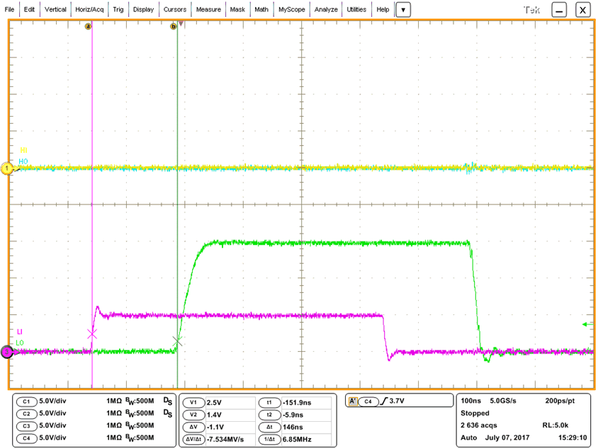 Figure 48. LI to LO Turn-On Propagation Delay
 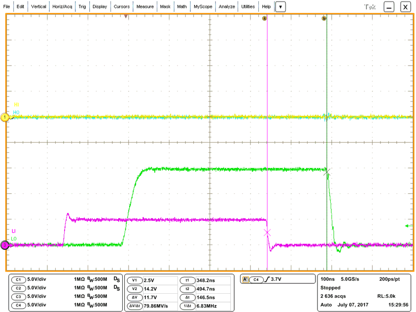 Figure 49. LI to LO Turn-Off Propagation Delay
 Figure 50 and Figure 51 show the measured HI to HO turn-on and turn-off delay of one UCC27710 device. Channel 1 depicts HI and Channel 2 HO.
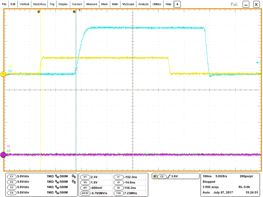 Figure 50. HI to HO Turn-On Propagation Delay
 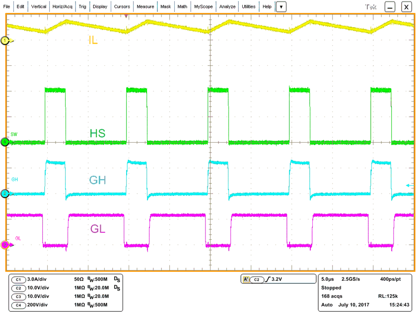 Figure 52. MOSFET Sync-Buck Operating at 400 V and 150 W
 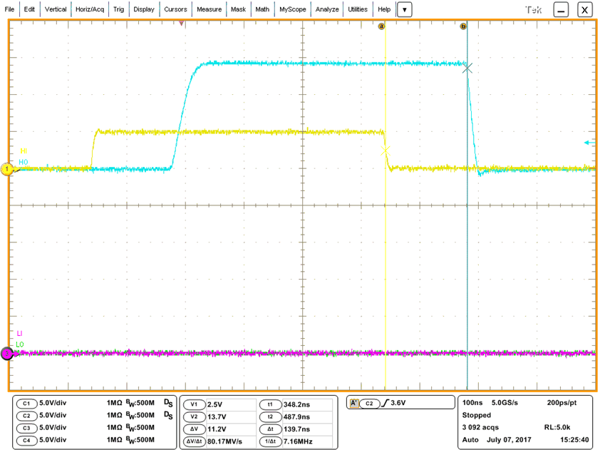 Figure 51. HI to HO Turn-Off Propagation Delay
 Figure 52 shows UCC27710 operating in a high voltage sync-buck. Channel 1 depicts inductor current, Channel 2 high side MOSFET VGS, Channel 3 low side MOSFET VGS, and Channel 4 high voltage switch node.