SBAU336A March   2020  – March 2021 AMC3306M05 , AMC3306M25 , AMC3336 , AMC3336-Q1


  1.   Trademarks
  2. 1EVM Overview
    1. 1.1 Features
    2. 1.2 Introduction
  3. 2Analog Interface
    1. 2.1 Analog Inputs
    2. 2.2 Digital Input and Output
  4. 3Power Supplies
    1. 3.1 VDD Input
  5. 4EVM Operation
    1. 4.1 Analog Inputs: J2
    2. 4.2 User Power and Digital Input and Output: J1 and J3
    3. 4.3 Device Operation
  6. 5Layout, BOM, and Schematic
    1. 5.1 Layout
    2. 5.2 Bill of Material
    3. 5.3 Schematic
  7.   Revision History

Layout

Figure 5-1 shows the AMC33xxEVM PCB layout.

Note:

Board layout is not to scale. This figure is intended to show how the board is laid out; it is not intended to be used for manufacturing AMC33xxEVM PCBs.
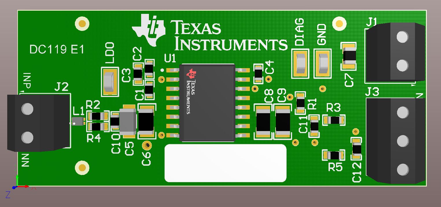
GUID-F3B444CC-F10F-4003-B56F-8BE7A8588C42-low.pngFigure 5-1 AMC33xxEVM Top Layer Silkscreen