SBOA505 December 2020 OPA2991-Q1 , TLV197-Q1 , TLV2197-Q1 , TLV4197-Q1 , TMP61 , TMP61-Q1 , TMP63 , TMP63-Q1 , TMP64-Q1
Design Description
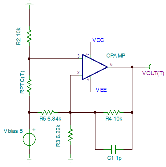
This temperature-sensing circuit uses minimal passive components and a single voltage source resulting in an ultra-small form factor. The circuit design allows for easy customization to accommodate various configurations and output voltage ranges. An operational amplifier (op amp) is used to offset and amplify the input signal as needed to utilize the full ADC range and improve measurement accuracy. The output of the PTC temperature sensor is fed to the non-inverting input of the amplifier, while a resistor network connected to high- and low-voltage sources offset the output as required.
The following figure shows the circuit schematic for the wide temperature NTC sensor.