SBOA505 December 2020 OPA2991-Q1 , TLV197-Q1 , TLV2197-Q1 , TLV4197-Q1 , TMP61 , TMP61-Q1 , TMP63 , TMP63-Q1 , TMP64-Q1
Design Simulations
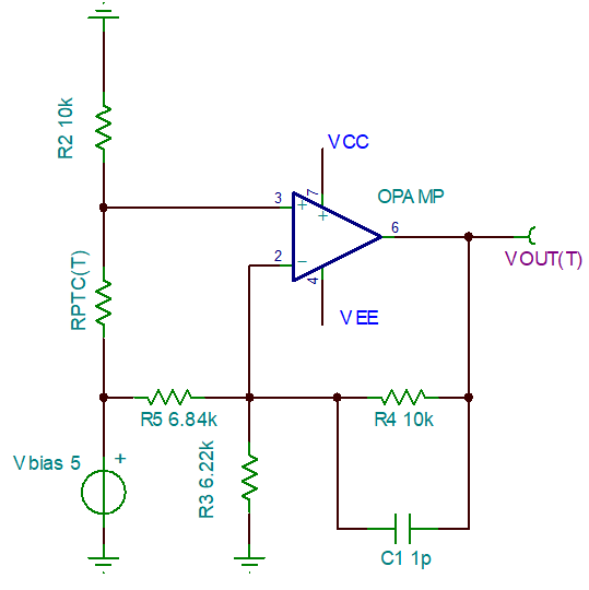
The following image shows the circuit schematic for the wide temperature NTC sensor circuit.
The TMP61 model was obtained via the reference design “ptc term foldback op amp mock” which is available for download from the design and development tab of the TMP61 Product Folder (SLOM480).
The TMP61 resistance across temperature response varies based on Vbias. The simulated PTC resistor must be edited in TINA-TI when changing Vbias to ensure the behavior matches the actual TMP61 values across temperature.
The temperature coefficients can be edited in the properties of the resistor.
The TMP61 lookup table is found in the Thermistor Design Tool (SBOC595).