SBOA505 December 2020 OPA2991-Q1 , TLV197-Q1 , TLV2197-Q1 , TLV4197-Q1 , TMP61 , TMP61-Q1 , TMP63 , TMP63-Q1 , TMP64-Q1
Improving Accuracy of the Sensor Circuit
- The temperature accuracy of the circuit can be
improved while continuing to use a linear
approximation to solve for the resistor network.
In this example the temperature range will be
optimized from 0°C to 90°C. This is accomplished
by decreasing the offset term of the
VOUT(T) equation.Equation 1.
- Recall, VOUT(T) is treated as a linear
equation to solve for the resistor network:
Equation 1.
- Therefore, the y-intercept, B, of the equation
can be used to offset the curve along the Y-Axis.
In this case the y-intercept of the equation
is:Equation 1.
- To shift the center of the
VOUT(T) curve the negative
inverting gain will be shifted 1.86%. The
1.86% shift was selected by calculating the
change needed to shift the midpoint of the
simulated VOUT(T) curve towards
the midpoint of the theoretical
VOUT(T) curve. The calculations needed to improve the accuracy of the NTC circuit are as follows:Equation 1.Equation 1.Equation 1.
- The new VOUT(T) can be obtained by
multiplying the ratio of R4 to R5 by 1.018 as
follows:Equation 1.Equation 1.Equation 1.
- The final resistor, R3, can be solved for using
the new R5 value. Note, this approach will
slightly affect the inverting gain of the circuit
however, the non-inverting gain of the circuit
will remain unchanged which will not impact the
gain of the voltage divider output voltage as a
function of temperature
(VNTC(T)).Equation 1.
- Using the linear approximation the resistor
network for the desired temperature range is as
follows:
R1 = 10kΩ
R2 = TMP61
R3 = 6.119kΩ
R4 = 10kΩ
R5 = 6.965kΩ
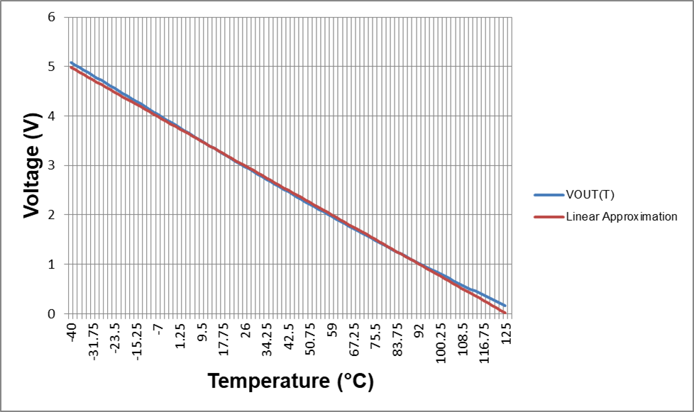
- Solving the resistor network for the optimized temperature range improved the accuracy across the overall temperature range of the sensor. The temperature error across the optimized temperature range is approximately 1.65°C which occurs at 49.1°C. The temperature reading from the ADC is approximately 50.75°C while the actual temperature is 49.1°C. However, the error at the end points increases.