SBOU187A april 2017 – april 2023 INA233
- Abstract
- Trademarks
- 1Overview
- 2INA233EVM Hardware
- 3INA233EVM Hardware Setup
-
4INA233EVM Software Overview
- 4.1 Starting the INA233EVM Software
- 4.2 Configuring the INA233EVM Software
- 4.3 Using the INA233EVM Software
- 5INA233EVM Documentation
- 6Revision History
4.2.1 I2C Address Selection
The INA233 device has a flexible I2C address configuration that allows for multiple devices to be on the same I2C lines. By moving the A0 and A1 addresses on jumpers J1 and J2 to either GND, VS, SDA, or SCL, the INA233 can be changed to a total of 16 I2C addresses as shown in Table 4-1.
| A1 | A0 | Slave Address | Corresponding I2C Address in the GUI |
|---|---|---|---|
| GND | GND | 1000000 | Read: x81 Write: x80 |
| GND | VS | 1000001 | Read: x83 Write: x82 |
| GND | SDA | 1000010 | Read: x85 Write: x84 |
| GND | SCL | 1000011 | Read: x87 Write: x86 |
| VS | GND | 1000100 | Read: x89 Write: x88 |
| VS | VS | 1000101 | Read: x8B Write: x8A |
| VS | SDA | 1000110 | Read: x8D Write: x8C |
| VS | SCL | 1000111 | Read: x8F Write: x8E |
| SDA | GND | 1001000 | Read: x91 Write: x90 |
| SDA | VS | 1001001 | Read: x93 Write: x92 |
| SDA | SDA | 1001010 | Read: x95 Write: x94 |
| SDA | SCL | 1001011 | Read: x97 Write: x96 |
| SCL | GND | 1001100 | Read: x99 Write: x98 |
| SCL | VS | 1001101 | Read: x9B Write: x9A |
| SCL | SDA | 1001110 | Read: x9D Write: x9C |
| SCL | SCL | 1001111 | Read: x9F Write: x9E |
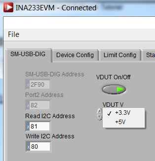
Figure 4-3 illustrates how to configure the I2C addresses. To configure the I2C address in the GUI navigate to the SM-USB-DIG tab. Click on the Read I2C Address and Write I2C Address to input the I2C address configured on the INA233EVM hardware. Refer to Table 4-1 to make sure you assign the correct values.
 Figure 4-3 Setting
the I2C Address