SBOU187A april   2017  – april 2023 INA233


  1.   Abstract
  2.   Trademarks
  3. 1Overview
    1. 1.1 INA233EVM Kit Contents
    2. 1.2 Related Documentation from Texas Instruments
  4. 2INA233EVM Hardware
    1. 2.1 Theory of Operation for INA233 Hardware
    2. 2.2 Signal Definitions of H1 (10-Pin Connector Socket)
      1. 2.2.1 SM-USB-DIG Platform Description
  5. 3INA233EVM Hardware Setup
    1. 3.1 Electrostatic Discharge Warning
    2. 3.2 One-Time INA233EVM GUI Software Setup
      1. 3.2.1 Hardware Requirements
      2. 3.2.2 Software Installation
    3. 3.3 Configuration of INA233EVM Jumper Settings
    4. 3.4 Connecting the Hardware
      1. 3.4.1 System Power Up
    5. 3.5 INA233EVM Features
      1. 3.5.1 J3: I2C VS Control Setting
      2. 3.5.2 J1: I2C Address Hardware Setting (A0)
      3. 3.5.3 J2: I2C Address Hardware Setting (A1)
      4. 3.5.4 External I2C Lines and Test Points SCL and SDA
      5. 3.5.5 IN+/IN– Input Filter (R1, R2, and C1)
      6. 3.5.6 Shunt Monitor Configuration
  6. 4INA233EVM Software Overview
    1. 4.1 Starting the INA233EVM Software
    2. 4.2 Configuring the INA233EVM Software
      1. 4.2.1 I2C Address Selection
      2. 4.2.2 Set the Configuration Register (MFR_ADC_CONFIG)
        1. 4.2.2.1 Set Averaging Mode
        2. 4.2.2.2 Set Conversion Times
        3. 4.2.2.3 Set Operating Mode
      3. 4.2.3 Set Calibration Register (MFR_CALIBRATION)
      4. 4.2.4 Set the MFR_DEVICE_CONFIG Register
      5. 4.2.5 Set the MFR_ALERT_MASK
      6. 4.2.6 Set the Warning Limit Registers
    3. 4.3 Using the INA233EVM Software
      1. 4.3.1 Read Data Tab
      2. 4.3.2 Status Register Tab
      3. 4.3.3 Register Map Tab
      4. 4.3.4 Plots Tab
  7. 5INA233EVM Documentation
    1. 5.1 Schematic
    2. 5.2 PCB Layout
    3. 5.3 Bill of Materials
  8. 6Revision History

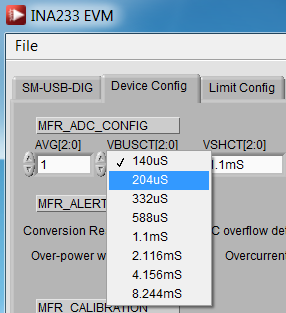
Set Conversion Times

Setting the conversion times allows the user to customize the amount of measurement time for conversions. Typically, for the INA233EVM software, the user is not able to notice a visual difference between the conversion times unless a high averaging mode and conversion time are chosen. The Shunt and Bus conversion times can be set as shown in Figure 4-5.
GUID-1AEA63B7-380E-498C-9DBA-D06380CF0BB6-low.pngFigure 4-5 Configuring Conversion Times