SLAA890A December 2019 – August 2021 MSP430FR2000 , MSP430FR2032 , MSP430FR2033 , MSP430FR2100 , MSP430FR2110 , MSP430FR2111 , MSP430FR2153 , MSP430FR2155 , MSP430FR2310 , MSP430FR2311 , MSP430FR2353 , MSP430FR2355 , MSP430FR2422 , MSP430FR2433 , MSP430FR2475 , MSP430FR2476 , MSP430FR2512 , MSP430FR2522 , MSP430FR2532 , MSP430FR2533 , MSP430FR2632 , MSP430FR2633 , MSP430FR2672 , MSP430FR2673 , MSP430FR2675 , MSP430FR2676 , MSP430FR4131 , MSP430FR4132 , MSP430FR4133
- Trademarks
- 1Overview of the MSP430FR4xx and MSP430FR2xx ADC Module
- 2Comparison Between the FR2xx/FR4xx ADC and ADC12_B
- 3Tailoring the ADC and Reference Voltages to Your Application
- 4Using the Window Comparator to Monitor a Signal Without CPU Intervention
- 5Calibration of VREF and the Internal Temperature Sensor to Improve Performance
- 6FR2xx/FR4xx ADC Example Code and Resources
- 7References
- 8Revision History
3.1 Reference Voltages
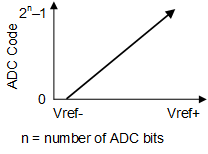
A reference voltage is a fixed voltage that ideally should not have any temperature- or supply-dependent variations. An ADC requires a reference voltage that has a negative and positive side as a reference point for the ADC input signal. The ADC then translates the input signal to a digital value (ADC code) based on the signal relative to the reference voltage. The application code deciphers the ADC code in reference to the input signal voltage. Figure 3-1 shows a linear translation graph of a reference voltage to an ADC code.
 Figure 3-1 Input Signal Voltage vs ADC Code
The maximum ADC code value is calculated by (2n – 1) where n is the number of ADC resolution bits. The positive side of the reference voltage translates to the highest ADC code. If an input signal is higher than the reference voltage, the measurement is then saturated to the maximum ADC code value. For example, if the ADC is 12 bits, the maximum ADC code is (212 – 1) = 4095 injecting a voltage above the device specification into the ADC pins can cause permanent damage to the pin or the device itself. For more information, see the data sheet parameter on analog input voltage range. For measuring voltages that exceed the input range of the ADC, external circuitry can be required to adjust external voltage to the optimal ADC input range (for example, voltage dividers or amplifiers).