SLAA890A December 2019 – August 2021 MSP430FR2000 , MSP430FR2032 , MSP430FR2033 , MSP430FR2100 , MSP430FR2110 , MSP430FR2111 , MSP430FR2153 , MSP430FR2155 , MSP430FR2310 , MSP430FR2311 , MSP430FR2353 , MSP430FR2355 , MSP430FR2422 , MSP430FR2433 , MSP430FR2475 , MSP430FR2476 , MSP430FR2512 , MSP430FR2522 , MSP430FR2532 , MSP430FR2533 , MSP430FR2632 , MSP430FR2633 , MSP430FR2672 , MSP430FR2673 , MSP430FR2675 , MSP430FR2676 , MSP430FR4131 , MSP430FR4132 , MSP430FR4133
- Trademarks
- 1Overview of the MSP430FR4xx and MSP430FR2xx ADC Module
- 2Comparison Between the FR2xx/FR4xx ADC and ADC12_B
- 3Tailoring the ADC and Reference Voltages to Your Application
- 4Using the Window Comparator to Monitor a Signal Without CPU Intervention
- 5Calibration of VREF and the Internal Temperature Sensor to Improve Performance
- 6FR2xx/FR4xx ADC Example Code and Resources
- 7References
- 8Revision History
3.5 Clock Selection
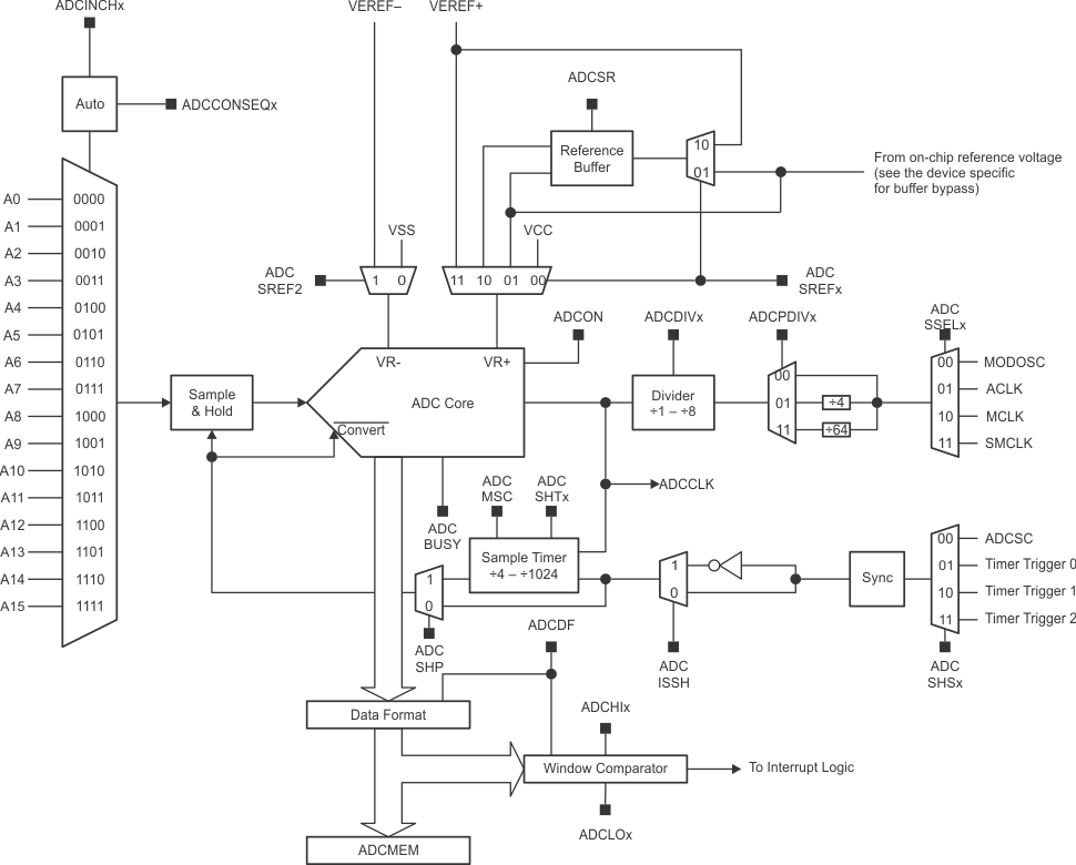
The ADC requires a clock source to convert the sampled analog input pin to an ADC code. The ADC conversion time is specified as (N + 2) × 1/fADCCLK in the device-specific data sheet. According to the MSP430FR4xx and MSP430FR2xx Family User's Guide, ADC clock can be selected from among MODOSC, ACLK, MCLK, and SMCLK as Figure 3-4 shows.

The ADC clock frequency range and the MODOSC frequency are specified in the device-specific data sheet. According to the ADC timing parameters in the MSP430FR235x, MSP430FR215x data sheet, the ADC clock frequency for 12-bit mode should be less than or equal to 4.4 MHz, and the MODOSC frequency range is 3.0 to 4.6 MHz according to Table 3-4.
| PARAMETER | DEVICE GRADE | VCC | MIN | TYP | MAX | UNIT | |
|---|---|---|---|---|---|---|---|
| fMODOSC | MODOSC frequency | T | 3.0 V | 3.0 | 3.8 | 4.6 | MHz |
| fMODOSC/dT | MODOSC frequency temperature drift(1) | T | 3.0 V | 0.102 | %/℃ | ||
| fMODOSC/dVCC | MODOSC frequency supply voltage drift | T | 1.8 V to 3.6 V | 1.17 | %/V | ||
| fMODOSC,DC | Duty cycle | T | 3.0 V | 40% | 50% | 60% | |
The previous example is for the MSP430FR2355. If the ADC clock is set to 4 MHz with SMCLK, the ADC sample-and-hold time is set to 4 ADCCLK cycles by the ADCSHTx bits in the ADCCTL0 register. The ADC conversion time is specified as (N + 2) × 1/fADCCLK. tSettling is 100 ns. Therefore, one complete ADC time would be 4 / 4 MHz + 14 / 4 MHz + 100 ns = 4.6 µs, and the ADC sample-and-hold rate is 217 ksps. If the ADC clock is set to MODOSC at approximately 3.8 MHz, the ADC sample-and-hold rate is 207 ksps, using the same calculation method.