SLAT161 June   2022 HD3SS3411 , TMUXHS4412


  1.   Abstract
  2.   Trademarks
  3. 1Introduction
  4. 2What is PCI Express (PCIe)?
    1. 2.1 PCIe Link
    2. 2.2 PCIe Clocking Architectures
      1. 2.2.1 Common Reference Clock
      2. 2.2.2 Data Reference Clock
      3. 2.2.3 Separate Reference Clock
    3. 2.3 PCIe Reference Clock Specification
  5. 3Reference Clock Measurement With TI Multiplexers
    1. 3.1 Test Setup and Procedure
      1. 3.1.1 Test Setup
      2. 3.1.2 Test Procedure
    2. 3.2 Test Report
      1. 3.2.1 Test Result With Clock Source
      2. 3.2.2 Test Result With HD3SS3411
      3. 3.2.3 Test Result With TMUXHS4412
      4. 3.2.4 Test Result With TMUXHS221
  6. 4Summary

Data Reference Clock

Figure 2-3 shows the Data refclk architecture. The Data refclk architecture is the simplest to implement since it only requires one clock source located at the transmitter. Although the Data refclk architecture has a simpler block diagram, its jitter requirements are more difficult to meet because less filtering is applied. The data refclk architecture is only supported in PCIe Gen 2 and Gen 3.
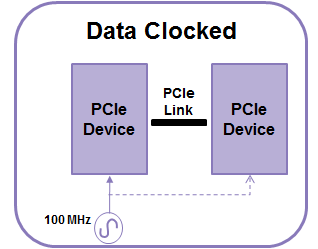
GUID-20220628-SS0I-GWZD-RK1F-DXPWVJGBKGJS-low.png Figure 2-3 Data Clock Architecture