SLAT161 June   2022 HD3SS3411 , TMUXHS4412


  1.   Abstract
  2.   Trademarks
  3. 1Introduction
  4. 2What is PCI Express (PCIe)?
    1. 2.1 PCIe Link
    2. 2.2 PCIe Clocking Architectures
      1. 2.2.1 Common Reference Clock
      2. 2.2.2 Data Reference Clock
      3. 2.2.3 Separate Reference Clock
    3. 2.3 PCIe Reference Clock Specification
  5. 3Reference Clock Measurement With TI Multiplexers
    1. 3.1 Test Setup and Procedure
      1. 3.1.1 Test Setup
      2. 3.1.2 Test Procedure
    2. 3.2 Test Report
      1. 3.2.1 Test Result With Clock Source
      2. 3.2.2 Test Result With HD3SS3411
      3. 3.2.3 Test Result With TMUXHS4412
      4. 3.2.4 Test Result With TMUXHS221
  6. 4Summary

Test Setup

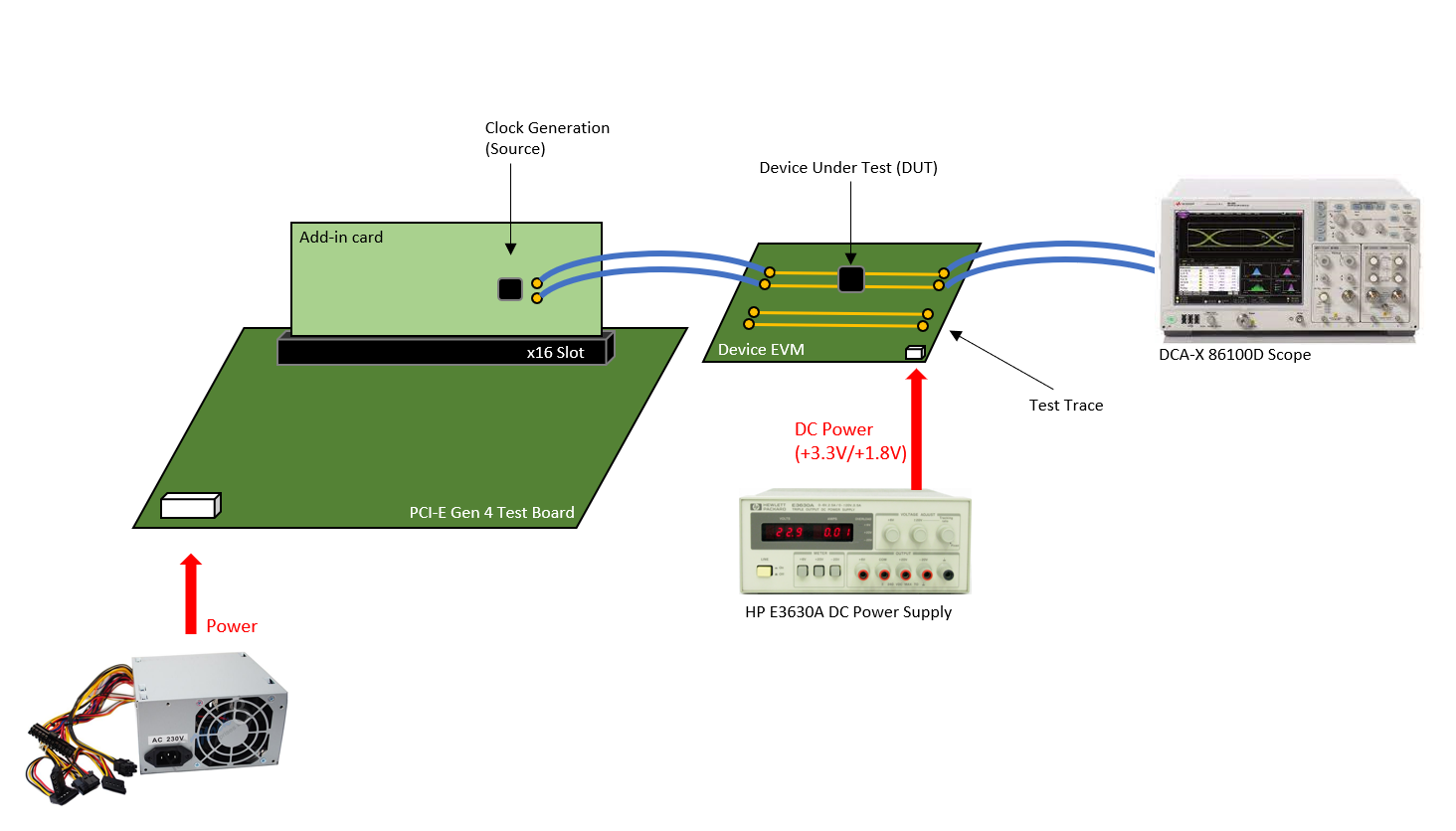
GUID-20220628-SS0I-Z91T-VF22-LFQ8P3GG6JSH-low.png Figure 3-1 Test Setup for PCIe Reference Clock Mesurement

Figure 3-1 is the setup for PCIe reference clock test. It includes:

  • 100 Mhz clock source (PCIe Add-in card)
  • EVMs of TMUXHS4412, TMUXHS221 and HD3SS3411
  • Power supply
  • DCA-X 86100D sampling scope