SLLA631A December 2023 – January 2024 UCC21220 , UCC21222-Q1 , UCC21520 , UCC21520-Q1 , UCC21530 , UCC21530-Q1 , UCC21540 , UCC21540-Q1
- 1
- Abstract
- Trademarks
- 1Introduction
- 2When Can Extreme Narrow Input Pulses Happen in a Power Stage?
- 3How Narrow Input Pulse Widths Threaten the Gate Driver
- 4Which System Factors Can Influence the Result
- 5How do you Know Whether Your System Should Limit Narrow Pulses?
- 6Summary
- 7References
- 8Revision History
5 How do you Know Whether Your System Should Limit Narrow Pulses?
The table below shows some common scenarios within the gate driver that can make the system design more susceptible to narrow pulses along with some mitigation tactics to consider.
| Gate Driver Scenarios Susceptible to Narrow Pulse | Mitigation | |
|---|---|---|
| Gate resistance (RG) | Having a low RG can lead to a higher di/dt. | Size RG to help limit the di/dt for the gate driver. |
| External VDD | Having a higher External VDD can leave lower margin in case of a narrow pulse that can exceed the absolute maximum rating for the device. | Consider limiting VDD range in the application. |
| Decoupling capacitor placement | Placing decoupling capacitors far away from the gate driver pins has a negative impact and can increase the parasitic trace inductance in the system. | Place decoupling capacitors as close the gate driver as possible to reduce parasitic inductance. Consult the TI data sheet for layout recommendations. |
As discussed in the previous section, the high coupled with parasitic inductance is the most important and easiest factor to control to avoid voltage spikes for narrow input commands. Extending the pulse width to make sure gate drive current has dropped close to zero can effectively minimize the change in current, .
One way to determine the minimum pulse width for your system is to monitor the MOSFET VGS voltage to decide whether the turn-ON or turn-OFF transition has completed. To make sure that negative impacts of narrow pulses do not cause damage to the gate driver, the primary recommendation is to have the driver output rise to higher than 90% of VDD before changing states again to achieve a Zero Current Switching for the turn-on.
In the case of a turn-off pulse, have the output fall to less than 10% of VDD before turning back on. This can make sure that large voltage spikes are not generated due to non-zero current switching of a high current in the presence of inductive parasitic on the PCB and in component package connections.
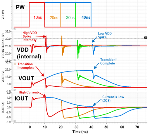
Figure 5-1 shows the relationship between VOUT, IOUT, Internal VDD of the gate driver, and a range of pulse widths to show the time required for a complete transition. In this example, the minimum pulse width of 40ns has IOUT low to achieve ZCS. In the case of 10ns pulse width, IOUT is being supplied near maximum output current and VOUT has not completed a full ON transition. The parasitic inductance can cause a high voltage spike internally to the gate driver that can cause the internal VDD to exceed the absolute maximum VDD voltage that the gate driver. Damage to the gate driver might not be seen immediately, but violating the absolute maximum ratings of the device can impact the integrity of the internal circuitry and degrade to the point of failure or physical damage to the IC induced from electrical overstress.
 Figure 5-1 Vout and VDD
Internal Voltage as on Pulse Extends