SLUAA61B September 2022 – November 2022 UCC27282-Q1 , UCC27284-Q1
1.1 Overview
This document contains information for UCC27282-Q1 UCC27284-Q1(SOIC and VSON package) to aid in a functional safety system design. Information provided are:
- Functional Safety Failure In Time (FIT) rates of the semiconductor component estimated by the application of industry reliability standards
- Pin failure mode analysis (Pin FMA)
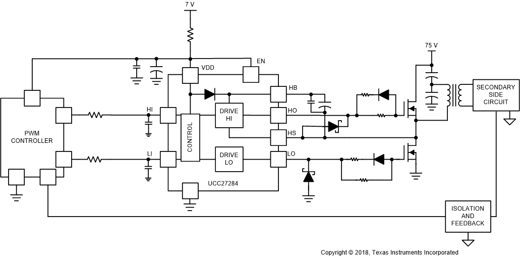
Figure 1-1 shows the device functional block diagram for reference.
 Figure 1-1 UCC27282-Q1
application Block diagram
 Figure 1-2 UCC27284-Q1
application Block diagram
Figure 1-2 UCC27284-Q1
application Block diagramUCC27282-Q1 UCC27284-Q1 were developed using a quality-managed development process, but was not developed in accordance with the IEC 61508 or ISO 26262 standards.