SLUAA61B September 2022 – November 2022 UCC27282-Q1 , UCC27284-Q1
1.3.2 VSON Package
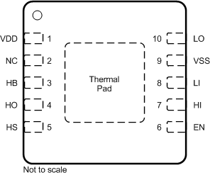
Figure 1-4 shows the UCC27282-Q1 pin diagram for the VSON package. For a detailed description of the device pins please refer to the 'Pin Configuration and Functions' section in the UCC27282-Q1 data sheet.
 Figure 1-4 Pin Diagram (VSON
Package)
Figure 1-4 Pin Diagram (VSON
Package)Table 1-12 Pin FMA for Device Pins Short-Circuited to Ground
| Pin Name | Pin No. | Description of Potential Failure Effect(s) | Failure Effect Class |
|---|---|---|---|
| VDD | 1 | LO will remain low. HO will remain low. | B |
| NC | 2 | No effect | D |
| HB | 3 | Device may be damaged with unknown LO/HO state | A |
| HO | 4 | Device may be damaged with unknown LO/HO state | A |
| HS | 5 | Device may be damaged with unknown LO/HO state | A |
| EN | 6 | LO will remain low. HO will remain low. | B |
| HI | 7 | HO will be in a low state | B |
| LI | 8 | LO will be a low state | B |
| VSS | 9 | No effect | D |
| LO | 10 | Device may be damaged with unknown LO/HO state | A |
Table 1-13 Pin
FMA for Device Pins Open-Circuited
| Pin Name | Pin No. | Description of Potential Failure Effect(s) | Failure Effect Class |
|---|---|---|---|
| VDD | 1 | LO will remain low. HO will remain low. | B |
| NC | 2 | No effect | D |
| HB | 3 | HO will be pulled to HS potential | B |
| HO | 4 | HO terminal not connected to the system | D |
| HS | 5 | HO will be pulled to HB potential | B |
| EN | 6 | LO will remain low. HO will remain low. | B |
| HI | 7 | HO will be in a low state | B |
| LI | 8 | LO will be in a low state | B |
| VSS | 9 | HO will be in a low state LO will be pulled to VDD | B |
| LO | 10 | LO terminal not connected to the system | D |
Table 1-14 Pin FMA for Device Pins Short-Circuited to Adjacent Pin
| Pin Name | Pin No. | Shorted to (PIN#+1) | Description of Potential Failure Effect(s) | Failure Effect Class |
|---|---|---|---|---|
| VDD | 1 | NC | No effect | D |
| NC | 2 | HB | No effect | D |
| HB | 3 | HO | Device may be damaged with unknown HO state | A |
| HO | 4 | HS | Device may be damaged with unknown LO/HO state | A |
| HS | 5 | N/A | - | - |
| EN | 6 | HI | LO/HO will follow the logic truth table per datasheet with EN in the same logic state as HI | B |
| HI | 7 | LI | HO/LO will be in a low state | B |
| LI | 8 | VSS | LO will be a low state | B |
| VSS | 9 | LO | Device may be damaged with unknown LO/HO state | A |
| LO | 10 | N/A | - | - |
Table 1-15 Pin FMA for Device Pins Short-Circuited to supply
| Pin Name | Pin No. | Description of Potential Failure Effect(s) | Failure Effect Class |
|---|---|---|---|
| VDD | 1 | No effect | D |
| NC | 2 | No effect | D |
| HB | 3 | Device may be damaged with unknown LO/HO state | A |
| HO | 4 | Device may be damaged with unknown LO/HO state | A |
| HS | 5 | Device may be damaged with unknown LO/HO state | A |
| EN | 6 | Short to 5V (I.E Power supply of the Microcontroller). LO/HO will follow the logic truth table per datasheet with EN stuck in a high state. | B |
| HI | 7 | Short to 5V (I.E Power supply of the Microcontroller) LO/HO will follow the interlock truth table depending on LI/HI | B |
| LI | 8 | Short to 5V (I.E Power supply of the Microcontroller) LO/HO will follow the interlock truth table depending on LI/HI | B |
| VSS | 9 | HO will be in a low state LO will be pulled to VDD | B |
| LO | 10 | Device may be damaged with unknown LO/HO state | A |