SLVAE30E February 2021 – March 2021 TPS1H000-Q1 , TPS1H100-Q1 , TPS1H200A-Q1 , TPS1HA08-Q1 , TPS25200-Q1 , TPS27S100 , TPS2H000-Q1 , TPS2H160-Q1 , TPS2HB16-Q1 , TPS2HB35-Q1 , TPS2HB50-Q1 , TPS4H000-Q1 , TPS4H160-Q1
- Trademarks
- 1Introduction
- 2Driving Resistive Loads
- 3Driving Capacitive Loads
- 4Driving Inductive Loads
- 5Driving LED Loads
- 6Appendix
- 7References
- 8Revision History
3.2 Application Examples
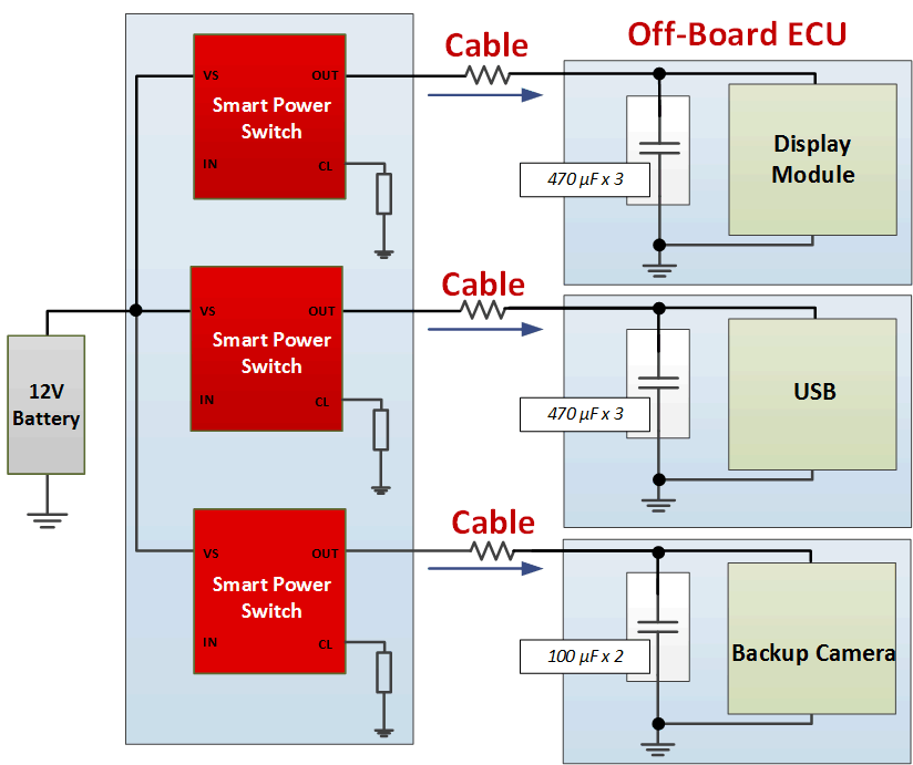
 Figure 3-1 Automotive Capacitive Load Driving Example
In automotive applications like Figure 3-1, many off-board ECUs have large bulk capacitances in place to stabilize the voltage at the input. As these modules must be able to reliably operate during input voltage drops, spikes, and switching noise, the capacitor bank is required to help prevent any loss of functionality. These capacitances can range from hundreds of microfarads up to millifarads.
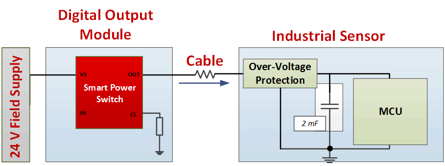
 Figure 3-2 Industrial Capacitive Load Driving Example
Industrial applications such as the PLC module seen in Figure 3-2 also must be able to drive large capacitive loads. Often digital output modules are used to provide power to sensors that are protected against transient surges. The easiest way to protect the sensor from this transient surge is to use an overvoltage switch that shuts off the sensor power during the overvoltage. This means that a large capacitance must be used to provide system power until the transient surge has passed and the overvoltage protection disengages. This large capacitance adds challenges to sensor start-up and can cause inrush current problems each time the over-voltage protection disengages. Without a careful design the inrush current can cause the 24-V external field supply voltage to droop which can blow fuses elsewhere in the system and cause dangerous reverse currents from other capacitive modules attached to the same supply.
In both of these examples it is necessary for the output designer to understand the impact of the capacitive load on the system and provide an effective, reliable, and efficient method to drive the loads. In the next sections we will investigate the challenges for reliably driving a capacitive load.