SLVAE30E February 2021 – March 2021 TPS1H000-Q1 , TPS1H100-Q1 , TPS1H200A-Q1 , TPS1HA08-Q1 , TPS25200-Q1 , TPS27S100 , TPS2H000-Q1 , TPS2H160-Q1 , TPS2HB16-Q1 , TPS2HB35-Q1 , TPS2HB50-Q1 , TPS2HC08-Q1 , TPS4H000-Q1 , TPS4H160-Q1
- Trademarks
- 1Introduction
- 2Driving Resistive Loads
- 3Driving Capacitive Loads
- 4Driving Inductive Loads
- 5Driving LED Loads
- 6Appendix
- 7References
- 8Revision History
3.3.4 Junction Temperature During Capacitive Inrush
The large thermal dissipation that a High Side Switch sustains during capacitive inrush can exceed the average power dissipation of the device calculated in Power Dissipation Calculation. This leads to relibaility concerns if device junction temperatures rise above Tj(Max) and possibly cause the device to go into Over Temperature Shutdown.
For average power consumption, we had estimated junction temperature as in Equation 4. Capacitive inrush events, however, are not steady-state conditions and are short in duration. A high-side switch may be able to tolerate higher-than-average power dissipation for short periods during inrush events due to the input-dependent thermal impedance.
Transient thermal impedance is typically modeled via a Foster RC network, shown in Figure 3-13. This model links the high-side switch junction temperature TJ to ambient temperature TA and the response of the thermal RC network to power dissipated in the device PDIS. The thermal impedance values in the model are strongly dependent on device construction and packaging. ZΘJA is defined as in Equation 25.
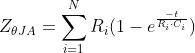
 Figure 3-13 Foster Network Model of Device
Thermal Impedance
Figure 3-13 Foster Network Model of Device
Thermal ImpedanceThis model shows us that short bursts of power have less effect on the junction temperature if the period is much less than the RC time constant, acting as a high-pass filter. For long periods of time, the thermal capacitances block the power and all the power passes through the thermal resistances R1,2,3..n. The sum of these thermal resistances in the model is RΘJA, which is specified in the device data sheets. The modeled response to a fast power transient is compared to a steady-state power dissipation in Figure 3-13.
 Figure 3-14 Effect of Thermal Time Constant on RΘJA and Junction Temperature
During capacitive inrush, ZΘJA, PDIS, and TJ are functions of time during, as shown in Figure 3-13. Time is on a logarithmic scale, and ZΘJA is the time dependent thermal impedance of the device (between junction and ambient air). ZΘJA follows an exponential decay according to the time constants of the Foster model for a particular device.
 Figure 3-15 RΘJA and Junction Temperature During an Inrush Period
ZΘJA is monotonically increasing during the inrush period, Δt, but total power dissipated in the device is dropping linearly due to current limiting. The peak power dissipation ILIM·VSUP occurs at the beginning of this period, while ZΘJA, the sum of decaying exponentials, peaks at the end of the inrush period.
This converse relationship causes junction temperature to peak at approximately half of the inrush period, or at Δt/2. This holds true as long the inrush period Δt is less than the effective thermal time constant of the device, or before ZΘJA plots flatten out. This is around 500 s for most high-side switches.
Mathematically, junction temperature is the convolution of ZΘJA and PDIS, which are both time variant, shown in Equation 26. Evaluating this convolution to find ΔTj is exceedingly difficult, and is best left to simulators like PSPICE if the device has a thermal-enabled model available.

Figures for transient thermal impedance ZΘJA are located in Appendix A and provided for each TI high-side switch listed in Table 3-1.
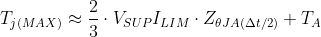
Equation 27 is accurate to within ±10% of PSPICE simulation results for TJ(Max), but only for inrush times Δt < ~500 s, or the point at which the ZΘJA curve flattens. Beyond this point, this approximation begins to undershoot as peak temperature occurs later than Δt/2. A more advanced thermal simulation with PSPICE, Simulink, or another modeling tool should be used at that point.
 from TPS2H160-Q1 Transient Thermal Impedance Curve") Figure 3-16 Estimating ZΘJA(Δt/2) from TPS2H160-Q1 Transient Thermal Impedance Curve
Figure 3-16 Estimating ZΘJA(Δt/2) from TPS2H160-Q1 Transient Thermal Impedance CurveThis procedure can be repeated for multi-channel devices using the transient thermal data ZΘJA for 2 or 4-Ch ON. However, this data should only be used for situations where both channels turn on simulatenously and the loading conditions are identical.
Adding on to our examples for TPS2H160-Q1, we can estimate TJ(Max) during capacitive inrush. In this example, a single channel drives a 470-µF capacitive load, current limit ILIM is set to 1 A, supply voltage is 24 V, and the ambient temperature is TA = 25°C.
From Equation 18, we found the inrush period lasts Δt = 11.28 ms. Referencing the data for TPS2H160-Q1 in Appendix A, we can draw a line at Δt = 11.28 ms as in Figure 3-16 to find the values of RΘJA at half the inrush period Δt since we are only driving on one channel, ZΘJA(Δt/2) = 5.4°C/W.
Current limiting is active during the inrush period and is responsible for significant power dissipation in the high-side switch. This is because current limiting is achieved through control of the FET RON. RON must be forced up to several orders of magnitude higher than the data sheet specification a the beginning of inrush, which leads to high I2R losses in the FET channel.
Once the device turns on the FET, VDS across the fet is initially VSUP and reduces to nearly 0 V once the capacitor load is charged. This initial point is where the peak power dissipation occurs. In our example with TPS2H160-Q1, we had set ILIM = 1 A, so the peak power is 24 V·1 A = 24W. We can now calculate TJ(MAX) during inrush by substituting our values for VSUP, ILIM, TA, and ZΘJA(Δt/2) into Equation 27, shown in Equation 28.

As this is an estimate and operating conditions may vary from the design point, it is recommended to allow for sufficient headroom between TJ(Max) and 150°C. Not properly limiting TJ may trigger over-temperature shutdown and reduce both reliability and device lifetime.
In addition to keeping TJ < 150°C, it is recommended to keep ΔTJ < TSW, where TSW = 60°C to prevent thermal swing shutdown during inrush. As the highest temperature will occur in the FET junction during inrush, designing for ΔTJ < TSW guarantees thermal swing shutdown will not be triggered during inrush. Since TFET TCON are strongly time-depenedent on loading conditions over inrush, ΔTJ could also potentially be larger than TSW without triggering thermal swing shutdown.
For the most accurate thermal results, it is strongly recommended to use thermal-enabled PSPICE models for TI's high-side switches which model TJ, TCON, and thermal shutdown. For more information on simulating device thermals in PSPICE, please see Using PSpice Simulator to Model Thermal Behavior in TI’s Smart High-Side Switches.