SLVAF59 April 2021 TPS2372 , TPS2373 , TPS23730 , TPS23731 , TPS23734 , TPS2375 , TPS2375-1 , TPS23750 , TPS23751 , TPS23752 , TPS23753A , TPS23754 , TPS23754-1 , TPS23755 , TPS23756 , TPS23757 , TPS23758 , TPS2376 , TPS2376-H , TPS2377 , TPS2377-1 , TPS23770 , TPS2378 , TPS2379
3.3 Secondary Side of the DCDC
This will highly depend on what the topology is.
In all topologies, the output component will probably need (or should have a footprint for) a snubber. The power rating, and thus size, of the resistor is very important. If the resistor is the incorrect value and size, it will either become a hot spot thermally, or whatever it is protecting will get hot. Additionally, the effective resistance may change because of the thermal condition, and then the snubber is no longer the correct value.
For all topologies, ensure there is enough output cap. The combination of ceramic and electrolytic is preferred. The ESR of an electrolytic or tantalum polymer cap will help set the dominate pole and zero in opto-feedback designs. This is less prevalent in PSR flybacks. If an inductor is used for filtering, the electrolytic capacitors need to be on the output side of the inductor. Only ceramics should be used on the input side because that side has much higher ripple currents, so the ripple rating and power rating of the electrolytic capacitors must account for this – but it is recommended to avoid that by placing them on the output side.
For diode flybacks: ensure the diode is the proper voltage and current rating for the output voltage and power level. Best to consult a reference design. But you can use the transformer turns ratio and output voltage and duty cycle to determine the proper voltage rating. Ensure there is a snubber across the output diode, and that snubber uses the appropriate component sizes. Additionally, ensure that the diode has a fast enough reverse recovery time, otherwise it can lead to lower efficiency.
 Figure 3-15 Diode Flyback: Output Diode
(and Snubber)
Figure 3-15 Diode Flyback: Output Diode
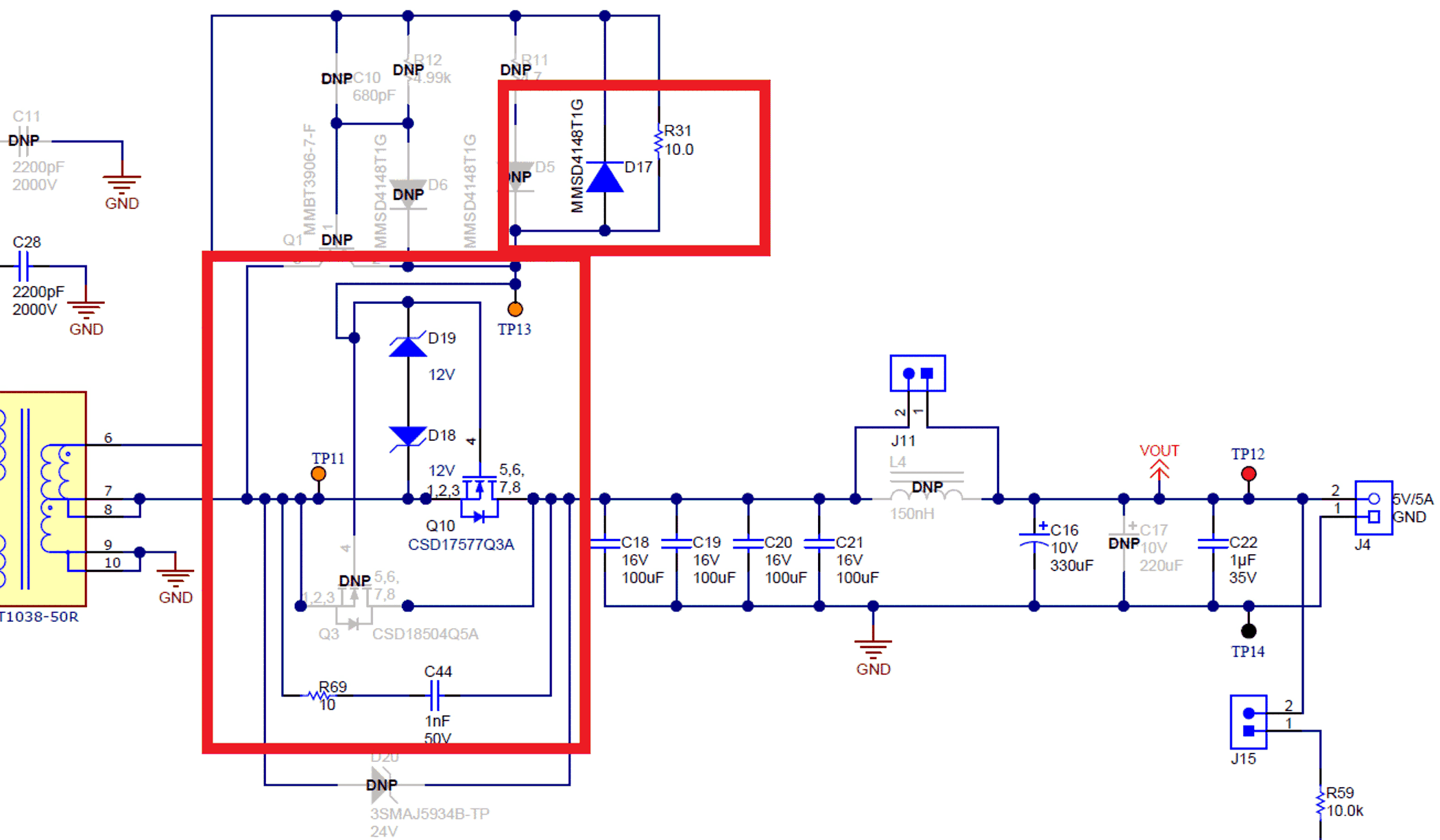
(and Snubber)For sync flybacks: There are multiple schemes for the grate drive of the FET. Some advice would be to look at a design with similar power and output voltage ratings to get appropriate parts. Sync flybacks are typically 5V and less. The TPS23753A has many designs for 13W and less, and the TPS23754/51 have many reference designs for 25W. Even if you are using the TPS2373x in a PSR design, the TPS23754 designs secondary gate drive is still valuable. For these gate drive components, size (power ratings, BJT package) and speed (reverse diode recovery time, diode capacitance) are everything. These gate drives turn off the FET fast which is important in reducing shoot through. The FET itself needs to be the appropriate Vds rating. The higher the output voltage, the higher the Vds voltage required (example, 5-V output 30-V-40-V; 12-Vout 60-V-100-V). Additionally, the gate charge needs to be as low as you can find. Some designs use back to back zeners, while others use a clamp to control the gate. Find an EVM and or reference design that you know works. If any changes are made, specially the transformer, then check the gate voltage during normal operation to see if back-to-back zeners work or if a clamp circuit is needed. If the gate voltage goes beyond the data sheet limit (usually -20V), then a clamp is suggested. If unsure, the gate clamp is more robust, but back-to-back zeners are smaller and less components. Typically the cost is about the same between the two solutions. Note, wide-Vin solutions might need to use the clamp circuit. If selecting the MOSFET, use the MOSFET in the EVM and or reference design as a base: the gate charge should be very similar (example, 21nC and 27nC are similar; 7nC and 18nC are not similar). Please note, this section does not go over the driven flyback that uses a pulse transformer to drive the secondary gate. For these designs, please follow the EVM and or reference design.
 Figure 3-16 Synchronous Flyback: Output
MOSFET (and Snubber)
Figure 3-16 Synchronous Flyback: Output
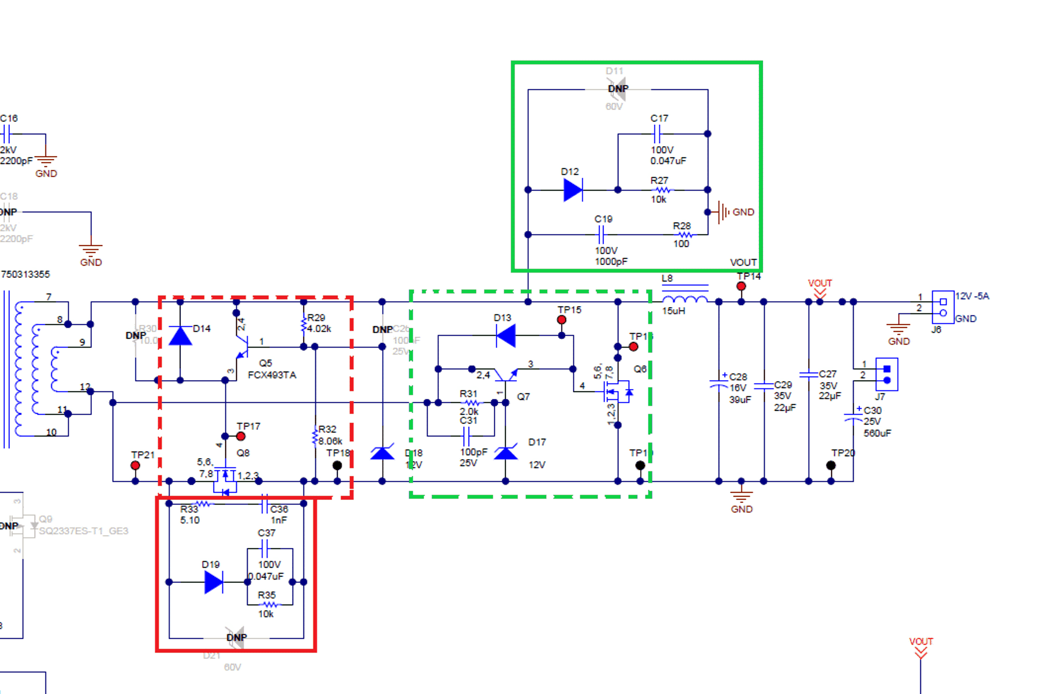
MOSFET (and Snubber)For Active Clamp Forwards: these are the most complex. This may appear obvious at this point, but the secondary is where it gets more complicated. The two MOSFETs are critical in the design, as well as the gate drive circuits. A quick note about the gate drive circuits. In 12-V output designs, a gate clamp is needed on both MOSFETs. In 5-V designs, the gate clamp is needed on the parallel. In <5-V designs, it is not needed on either. Since the two MOSFETs need to be working synchronously, the timing is more important than in a flyback. Choosing the appropriate MOSFETs and gate drive are important. In ACF designs, the MOSFETS need to switch very fast. Slow Rdson MOSFETs do not work. Ensure that the package size is greater than SOT-23, otherwise it will heat up. Additionally, these MOSFETs might need snubbers as well, ensure there is appropriate footprints for these components. It is suggested to find a similar reference design and copy the design. Please note that C31 can be critical for the efficiency and the turn-off voltage spike of the series MOSFET. In some situations, it helps, but in others, it does not. The factors of determining this is beyond what can be covered in this guide, but the suggestion is to strictly follow the presence of the capacitor if the capacitor is present or not in the reference design used. In Figure 3-17, the dotted boxes are the gate drives, and the solid boxes are the snubbers/clamps. The green is the parallel FET, and the red is the series FET.
The output inductor is required in the active clamp forward. The output inductor can be calculated.
 Figure 3-17 Active Clamp Forward Secondary
Side