SLVUC46D March 2021 – November 2023
2.2.7 Device Signal Test Points
The signals corresponding to each test point for both the hardware and SPI variant is given below for each of the devices. The naming convention for the test points is as follows: SPI/ HW. The signal on the test point for the SPI versions of the devices is listed first and then the HW variant.
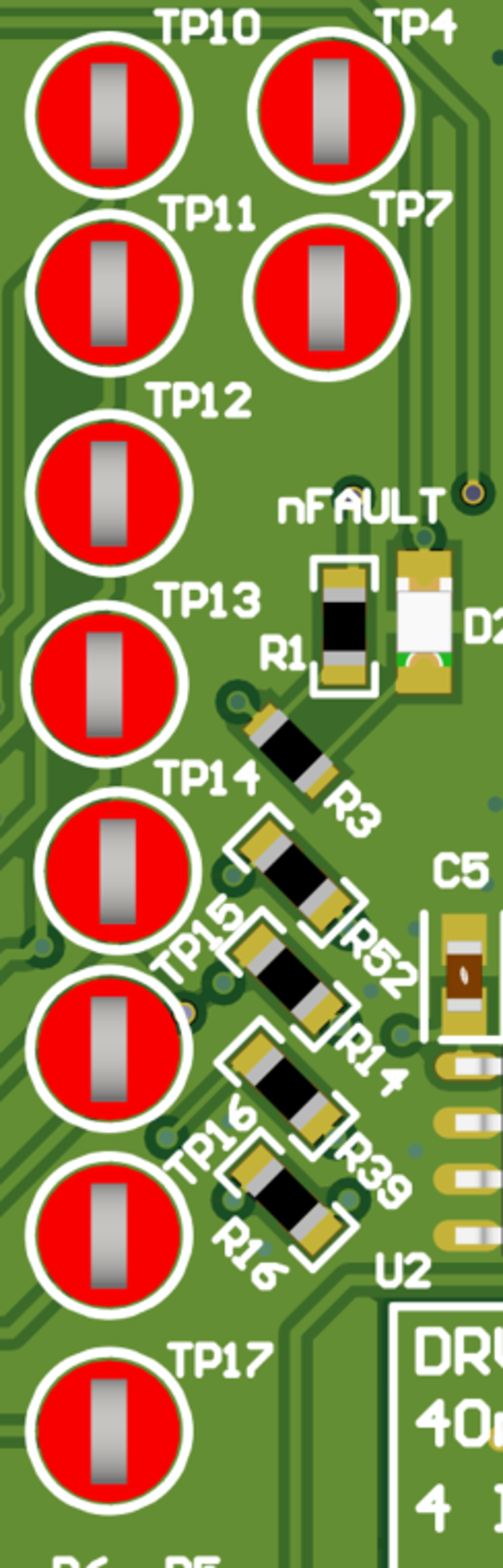
| Test Point number | DRV824x | DRV8145 |
|---|---|---|
| TP4 | nSLEEP | nSLEEP |
| TP7 | IPROPI | IPROPI |
| TP10 | nFAULT | nFAULT |
| TP11 | SDO/MODE | SDO/MODE |
| TP12 | SDI/ITRIP | SDI/ITRIP |
| TP13 | SCLK/SR | SCLK/SR |
| TP14 | nSCS/DIAG | nSCS/DIAG |
| TP15 | PH/IN2 | N/A |
| TP16 | EN/IN1 | EN/IN1 |
| TP17 | DRVOFF | EN/IN1 |
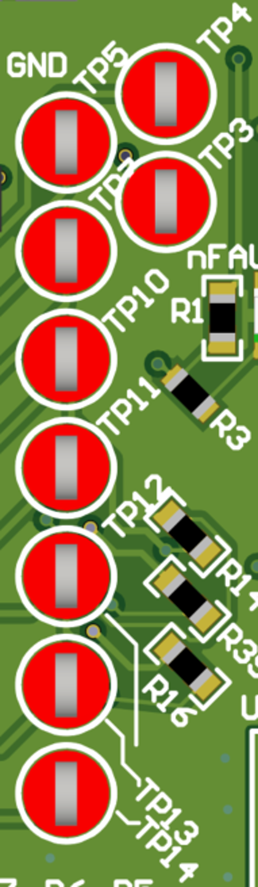
| Test Point number | DRV8144 |
|---|---|
| TP3 | nSLEEP |
| TP4 | IPROPI |
| TP5 | nFAULT |
| TP7 | SDO/NC |
| TP10 | SDI/ITRIP |
| TP11 | SCLK/SR |
| TP12 | nSCS/DIAG |
| TP13 | IN |
| TP14 | DRVOFF |