SLWU095 april 2023
3.3.3.3 JTAG Connectors
The TSW14J59EVM includes one industry-standard JTAG connector, P2, that connects to the JTAG port of the FPGA. The FPGA can be programmed using this connector or through the USB 3.0 interface. The USB 3.0 interface allows the FPGA to be programmed using the HSDC Pro software GUI. Every time the TSW14J59EVM is powered-down, the FPGA configuration is removed. The user must program the FPGA through the GUI after every time the board is powered-up. The FPGA can also be configured using the two on-board flash devices, U3 and U6.
The TSW14J59EVM also has a surface mount Digilent JTAG programmer, U5, which can be used to program the FPGA as well.
FLASH DEVICES The TSW14J59EVM includes two serial flash programming EEPROMS that can load FPGA firmware. Jumper J35 determines which EEPROM configures the FPGA when switch SW2 is pressed. If the EEPROMs are programmed, then, after power up, pressing SW2 loads the FPGA with the content of flash device U3 if J35 has a shunt between pins 1-2. The FPGA is programmed with the content of U6 if the shunt is between pins 2-3 or removed.
Program the Memory Device
To program U3 and U6 with new files, use the following steps:
- Connect the TSW14J59 Capture card to the PC through a JTAG Xilinx Programmer cable. This is the JTAG connect P2.
- Install a shunt on JP3.
- Open the Vivado Installation:
- Double click Open Hardware Manager.
- In the Hardware Manager, left click on Open target and select Auto Connect.
- The last step lists all the FPGAs connected to the PC through JTAG Programmer cables.
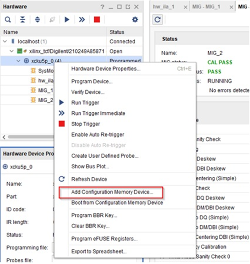
- Right click on “xcku5p_0” -> click on Add
Configuration Memory Device.
 Figure 3-1 Add Configuration
Memory Device
 - In the pop-up window, search for the “mt25qu256-spi-x1_x2_x4” component. Click the OK button.
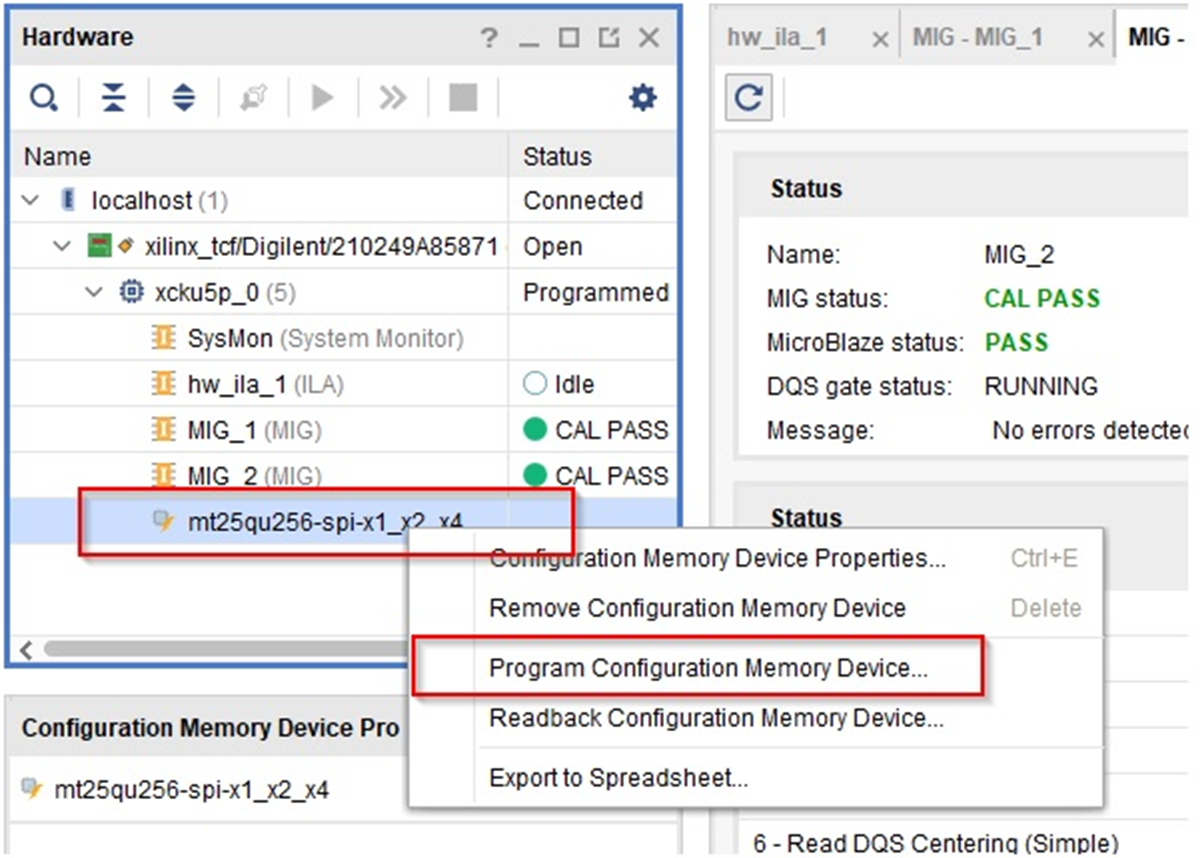
- Right click on device
“mt25qu256-spi-x1_x2_x4”, and click on Program Configuration Memory
Device (see Figure 3-2).
 Figure 3-2 Programming Memory
Device
 - To program U3, insert a
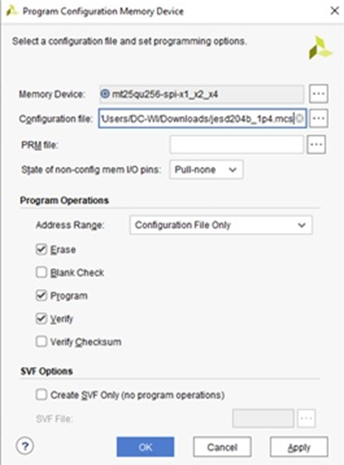
shunt on J35 pins 1–2, open up the new “xx.mcs” file to be loaded, and check the
following setup in the programming. Click the OK button when completed.
Figure 3-3 illustrates the configuration file to be loaded. If the file
loads properly, then a new message opens stating Flash programming completed
successfully. Click on the OK button.
 Figure 3-3 Config File
 - To program U6, place a shunt on J35 pins 2–3, open up the new “yy.mcs”file to be loaded and check the following setup in the programming. Click the OK button when completed.
- After the programing is completed, click on SW2, FPGA RESET, to load the image to the FPGA. With the shunt on pins 2-3 of J35, the image stored in U6 is loaded into the FPGA. With the shunt on 1-2 of J35, the image stored in U3 is loaded into the FPGA.