SNAU291 October   2023


  1.   1
  2.   Description
  3.   Features
  4.   Applications
  5.   5
  6. 1Evaluation Module Overview
    1. 1.1 Introduction
    2. 1.2 Kit Contents
    3. 1.3 Specification
    4. 1.4 Device Information
  7. 2Hardware
    1. 2.1 EVM Quick Start
      1. 2.1.1 Hardware Setup
      2. 2.1.2 EVM Measurements
    2. 2.2 Device Operation Modes
    3. 2.3 EVM Configuration
      1. 2.3.1 Power Supply
      2. 2.3.2 Logic Input and Outputs
      3. 2.3.3 Clock Input
      4. 2.3.4 Clock Outputs
      5. 2.3.5 Status Outputs, LEDs and Test Points
  8. 3Software
    1. 3.1 Software Installation
      1. 3.1.1 Software Setup
      2. 3.1.2 Program and Setup
    2. 3.2 TICS Pro LMKDB1108 Software
      1. 3.2.1 Input
        1. 3.2.1.1 Input Interface Type
        2. 3.2.1.2 Input Termination
        3. 3.2.1.3 Auto Output Disable (AOD)
        4. 3.2.1.4 LOS Event
        5. 3.2.1.5 LOS Readback
      2. 3.2.2 Device Info
        1. 3.2.2.1 EVM Setup
        2. 3.2.2.2 SMBus
      3. 3.2.3 Output
        1. 3.2.3.1 SMBus
        2. 3.2.3.2 OE Pin Control
        3. 3.2.3.3 Side Band Interface (SBI)
  9. 4Implementation Results
    1. 4.1 Typical Phase Noise Characteristic
  10. 5Hardware Design Files
    1. 5.1 Schematics
    2. 5.2 PCB Layouts
    3. 5.3 Bill of Materials (BOM)
  11. 6Compliance Information
    1. 6.1 Compliance and Certifications
  12. 7References

PCB Layouts


GUID-20231012-SS0I-DFLX-CZZH-TGTCPRP0VWQR-low.svg

Figure 5-9 Layer Stackup
GUID-20231012-SS0I-FDFQ-RTZH-LBDSHM7G6C5V-low.svg Figure 5-10 Top Layer (CLKIN / CLKOUT Signals)
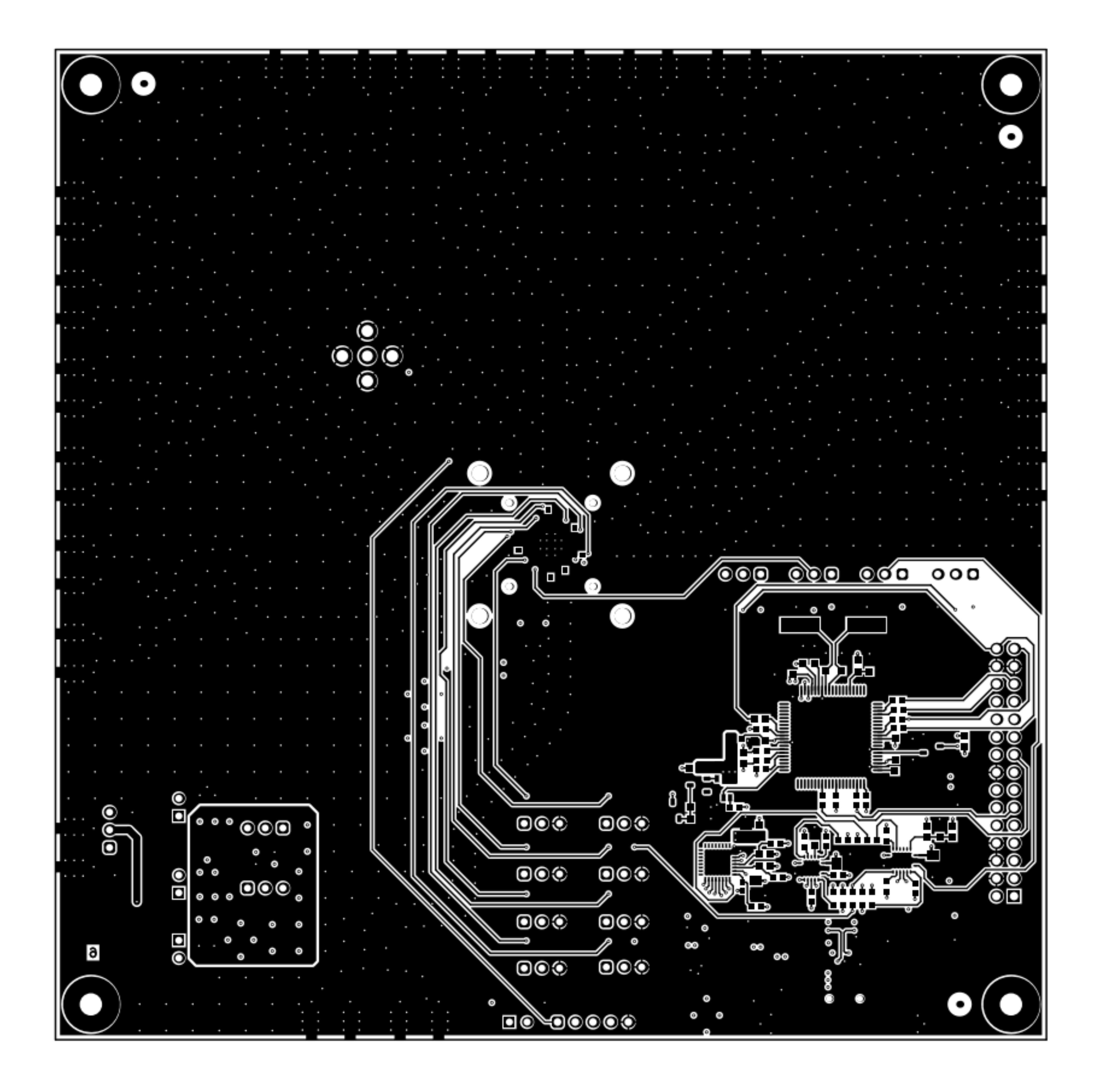
GUID-20231012-SS0I-JRW4-P6XD-WGDCCSCBQRDZ-low.png Figure 5-11 Bottom Layer
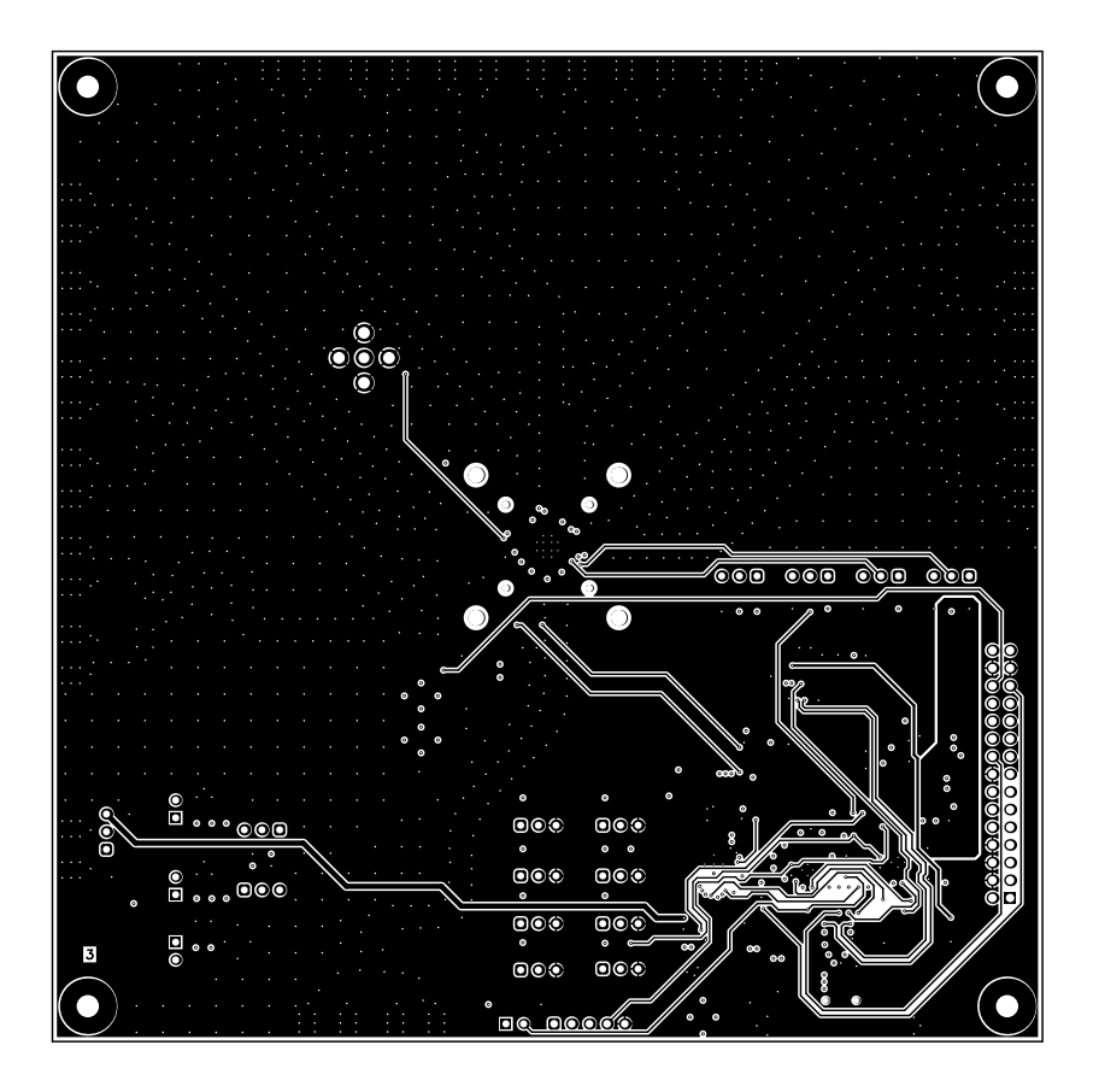
GUID-20231012-SS0I-NQWD-QDGX-WXKJHLZR0JT7-low.png Figure 5-12 Signal 1 Layer
GUID-20231012-SS0I-JQ9X-WZV6-VRMNTJST0BNH-low.svg Figure 5-13 PWR Layer
GUID-20231012-SS0I-NRS8-D9BJ-PJ6DSDFKH1LS-low.svg Figure 5-14 GND 1 Layer
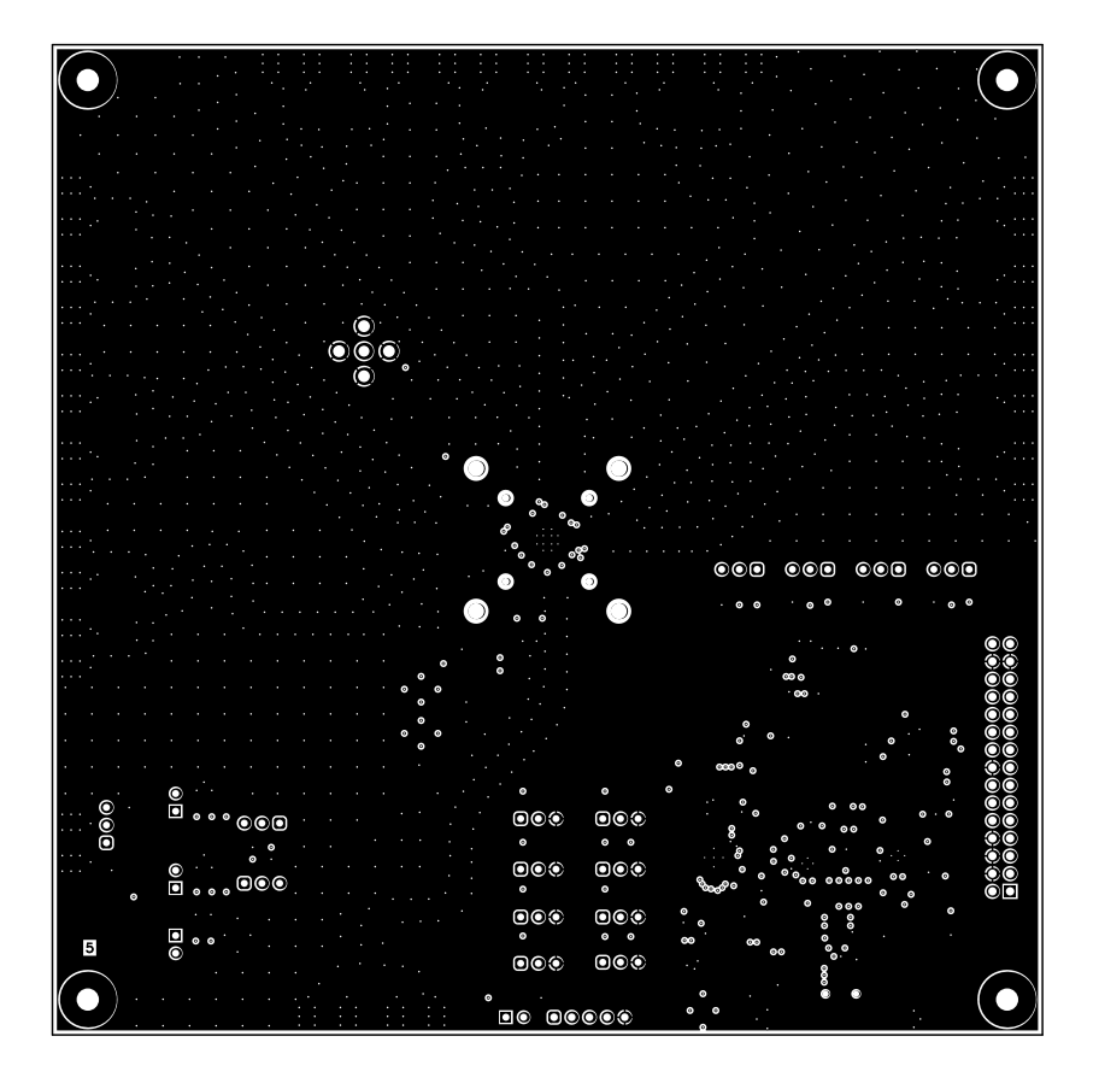
GUID-20231012-SS0I-7KFZ-FCH8-4RTSVZN4CSCC-low.png Figure 5-15 GND 2 Layer