SNLA437 December 2023 DP83822H , DP83822HF , DP83822I , DP83822IF , DP83825I , DP83826E , DP83826I
- 1
- Abstract
- Trademarks
- 1DP83822 Application Overview
-
2Troubleshooting the PHY Application
- 2.1 Schematic and Layout Checklist
- 2.2 Verify Successful Power-up of PHY
- 2.3 Read and Check Register Values
- 2.4 Peripheral Pin Checks
- 2.5 Verifying Strap Configurations During Initialization
- 2.6 Debugging Link Quality
- 2.7 Built-In Self Test With Various Loopback Modes
- 2.8 Debug the Fiber Connection
- 2.9 Debug the MAC Interface
- 2.10 Debug the Start of Frame Detect
- 2.11 Tools and References
- 3References
2.2 Verify Successful Power-up of PHY
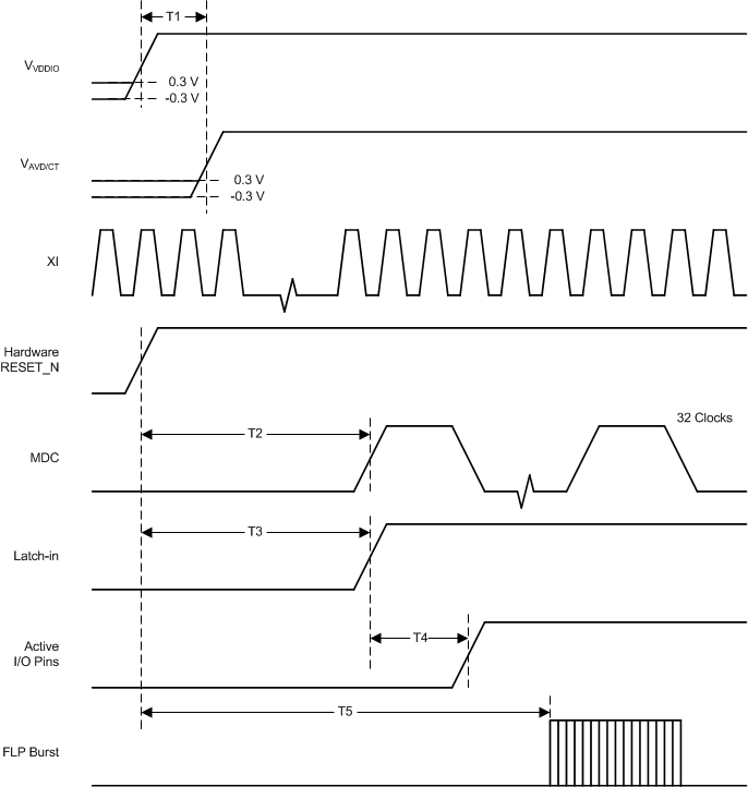
After verifying the schematics with the schematic checklist in the previous section, in order to start testing for any other issues that may present with application of the PHY, the PHY must first be successfully powered up in order to perform any other debugging processes. Probe the voltage rails of the PHY to ensure that the voltages are within limits defined in PHY Supply Voltage Specifications. Verify that the power up voltage parameter timings are within the limits defined in Timing Requirements, Power-Up Timing and Power-Up Timing.
| Descriptions | Min | Typ | Max | Unit | |
|---|---|---|---|---|---|
| VDDIO | Supply Voltage 1/O = 1.8V | 1.71 | 1.8 | 1.89 | V |
| Supply Voltage I/O = 2.5V | 2.375 | 2.5 | 2.625 | ||
| Supply Voltage I/O = 3.3V | 3.15 | 3.3 | 3.45 | ||
| AVD | Supply Voltage Analog = 3.3V | 3.15 | 3.3 | 3.45 | V |
| Supply Voltage Analog = 1.8V | 1.71 | 1.8 | 1.89 | ||
| Center Tap (CT) | Supply Voltage Center Tap = 3.3V | 3.15 | 3.3 | 3.45 | V |
| Supply Voltage Analog = 1.8V | 1.71 | 1.8 | 1.89 |
| Parameter | Test Conditions | MIN | TYP | MAX | Unit | |
|---|---|---|---|---|---|---|
| T1 | AVD (analog supply) ramp delay post VDDIO (digital
supply) ramp. AVD and VDDIO potential must not exceed 0.3 V prior to supply ramp. |
Time from start of supply ramp | –100 | 100 | ms | |
| VDDIO ramp time | 100 | ms | ||||
| AVD ramp time | 100 | ms | ||||
| T2 | Post power-up stabilization time prior to MDC
preamble for register accesses. MDC preamble coming in any time after this max wait time will be valid. |
MDIO is pulled high for 32-bit serial management initialization | 200 | ms | ||
| T3 | Hardware configuration latch-in time for power up | 200 | ms | |||
| T4 | Hardware configuration pins transition to output drivers | 64 | ns | |||
| T5 | Fast Link Pulse transmission delay post power up | 1.5 | s | |||
 Figure 2-1 Power-Up Timing
If a link up issue is present for DP83822 and the VDDA is operated in 3.3V, check register 0x0421 to see AVDD level and VDDIO level match the desire output. Register 0x0421 bit[2]=1 for 3.3V VDDA. If register 0x0421 does not match with the desire result, write 0x041F register to the desire voltage level. Write register 0x041F bit[12] = 1.
Registers 0x0421 and 0x041F are extended registers, make sure to follow Extended Register Access.