SPRAC31 February 2019 TMS320C5505 , TMS320C5515 , TMS320C5535
-
TMS320C5505/15/35/45 schematic checklist
- Trademarks
- 1 Introduction
- 2 Complimentary Resources
- 3
Recommendations Specific to C5504/05/14/15/32/33/34/35/45
- 3.1 Before You Begin
- 3.2 Unused Pins
- 3.3 Unused Power Rails
- 3.4 Clocking
- 3.5 OSC Internal Oscillator Clock Source
- 3.6 Power
- 3.7 Decoupling Capacitors
- 3.8 LDO Output Decoupling Capacitors
- 3.9 Digital GND, Analog GND, Local GND
- 3.10 Reset
- 3.11 USB
- 3.12 I2C
- 3.13 I2S
- 3.14 RTC
- 3.15 SAR ADC
- 3.16 Pin Muxing
- 3.17 Signal Visibility
- 3.18 EMIF (not applicable to C5532/33/34/35 or C5545)
- 3.19 JTAG
- 3.20 Bootloader
- 4 References
3.5 OSC Internal Oscillator Clock Source
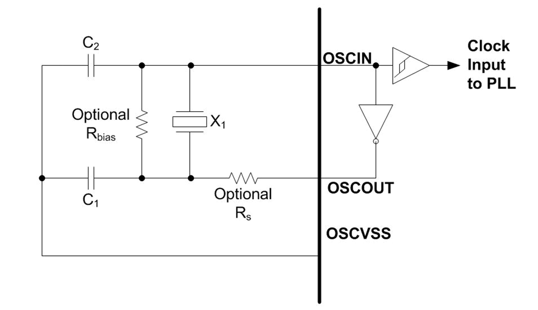
Figure 1 shows the recommended crystal circuit. It is recommended that pre-production printed circuit board (PCB) designs include the two optional resistors: Rbias and Rs. They may be required for proper oscillator operation when combined with production crystal circuit components
 Figure 1. OSC Crystal Circuit Schematics
 In general, adding Rbais and Rs resistors improves circuit performance by reducing the long start-up time, crystal overdrive and voltage and temperature related issues. Specifically, they provide the following functionality:
Rs helps reduce the drive level on the crystal and decreases the slew rate, which adds additional phase shift Recommended value: 50 Ω Rbais (the feedback resistor) is used to bias the input of the inverting amplifier and improve the loop gain Recommended value: 1M Ω. However, in most cases Rbias is not required and Rs is a 0-Ω resistor. These resistors may be removed from production PCB designs after evaluating oscillator performance with production crystal circuit components installed on pre-production PCBs.
For the calculation of Rs and RBais values, see the Crystek Application notes. Oscillator components (Crystal, C1, C2, optional Rbias and Rd) must be located close to the device package. Parasitic capacitance to the printed circuit board (PCB) ground and other signals should be minimized to reduce noise coupled into the oscillator.