SPRUJ63A September 2022 – October 2023
- 1
- Trademarks
- 1Introduction
- 2Important Usage Notes
-
3System Description
- 3.1 Key Features
- 3.2 Functional Block Diagram
- 3.3 Power-On/Off Procedures
- 3.4
Peripheral and Major Component
Description
- 3.4.1 Clocking
- 3.4.2 Reset
- 3.4.3 Power
- 3.4.4 Configuration
- 3.4.5 JTAG
- 3.4.6 Test Automation
- 3.4.7 UART Interfaces
- 3.4.8 Memory Interfaces
- 3.4.9 Ethernet Interface
- 3.4.10 Display Interface
- 3.4.11 USB 2.0 Interface
- 3.4.12 PCIe Interface
- 3.4.13 High Speed Expansion Interface
- 3.4.14 CAN Interface
- 3.4.15 Interrupt
- 3.4.16 ADC Interface
- 3.4.17 Safety Connector
- 3.4.18 SPI Interfaces
- 3.4.19 I2C Interfaces
- 3.4.20 FSI Interface
- 4Known Issues and Modifications
- 5References
- 6Revision History
3.4.9.2 DP83869 PHY Default Configuration
The DP83869 PHY uses four level configurations for I/O, RX_D0 and RX_D1 pins and two-level configurations for all other pins. The four level strap pins based on resistor strapping generates four distinct voltages ranges. The resistors are connected to the RX data pins, which are normally driven by the PHY and are inputs to the AM64x/AM243x. The voltage range for each mode is shown below:
Mode 0 - 0 V to 0.3069 V
Mode 1 – 0.4488 V to 0.6072 V
Mode 2 – 0.7227 V to 0.924 V
Mode 3 – 1.98 V to 2.9304 V
The two level strap pins based on resistor strapping generates two distinct voltage ranges. The resistors are connected to the LED pins. Because the LED output pins are also used as straps, the external components required for strapping and LED usage must be considered to avoid contention. Specifically, this can be an issue when the LED outputs are used to drive LED directly. The voltage range for each mode is shown below:
Mode 0 - 0 V to 0.594 V
Mode 1 – 1.65 V to 2.904 V
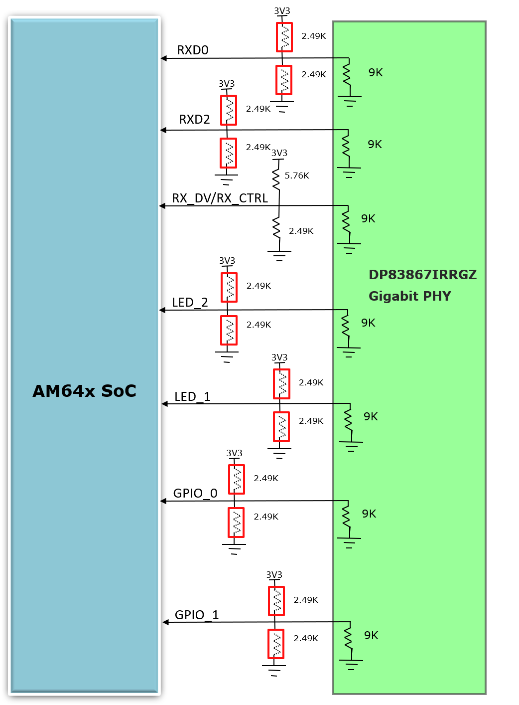
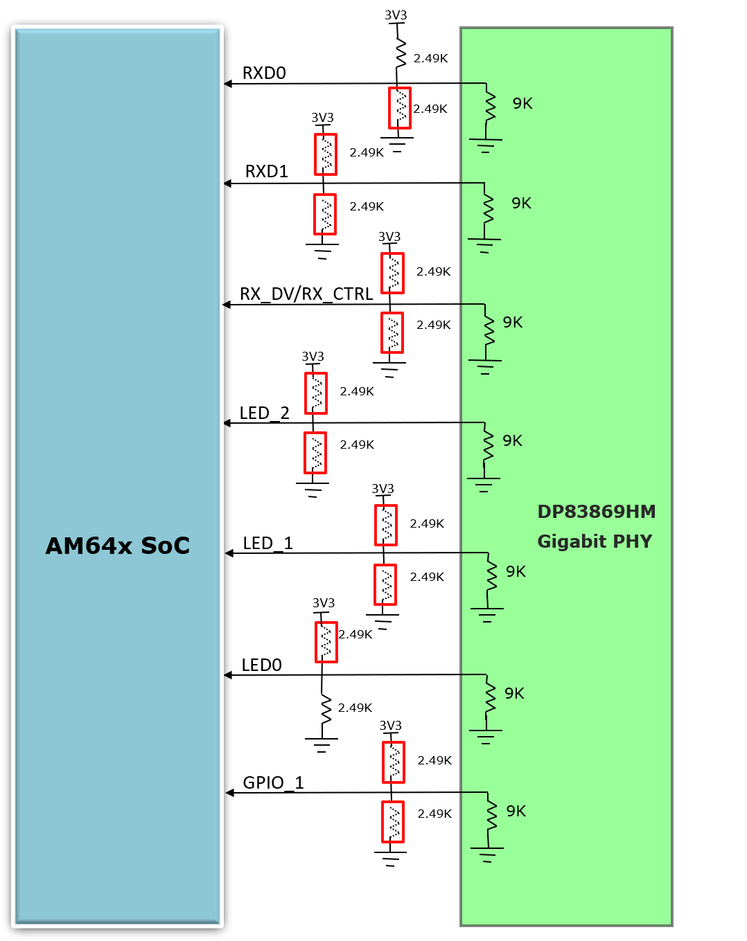
DP83869 device includes internal pull-down resistor. The value of the external pull resistors is selected to provide voltage at the pins of the AM64x/AM243x as close to ground or 3.3 V as possible. The strapping is shown in Figure 3-21 and the strap values are given in Table 3-20.
Address strapping is provided for ICSSG1 PHY to set address of 00011 (03h) and ICSSG2 PHY to set address of 01111 (0Fh) using the strap resistors. Footprint for both pull up and pull down is provided on all the strapping pins.
| Strap Setting | Pin Name | Strap Function | Mode for PRG0_PRU1, PRG0_PRU0, PRG1_PRU1, PRG1_PRU0 | Value of Strap Function for PRG0 and PRG1 | Description |
|---|---|---|---|---|---|
| PHY Address | RX_D2 | PHY_AD3 | 1 | 0 | PHY Address: 0000 |
| PHY_AD2 | 1 | 0 | |||
| RX_D0 | PHY_AD1 | 1 | 0 | ||
| PHY_AD0 | 1 | 0 | |||
| Auto Negotiation | RX_DV/RX_CTRL | Auto-neg | 3 | 0 | Auto neg Disable=0 |
| Modes of Operation | LED_2 | RGMII Clock Skew TX[1] | 1 | 0 | RGMII TX Clock Skew is set to 2 ns |
| RGMII Clock Skew TX[0] | 1 | 0 | |||
| LED_1 | RGMII Clock Skew TX[2] | 1 | 0 | ||
| ANEG_SEL | 1 | 0 | advertise ability of 10/100/1000 | ||
| LED_0 | Mirror Enable | 1 | 0 | Mirror Enable Disabled | |
| GPIO_1 | RGMII Clock Skew RX[2] | 1 | 0 | RGMII RX Clock Skew is set to 2 ns | |
| RGMII clock Skew TX[1] | 1 | 0 | |||
| GPIO_0 | RGMII clock Skew RX[0] | 1 | 0 |
| Strap Setting | Pin Name | Strap Function | Mode for PRG1_RGMII2 (ICSSG1) | Value of Strap Function for PRG1_RGMII2 (ICSSG1) | Mode for PRG1_RGMII1 (ICSSG2) | Value of Strap Function for PRG1_RGMII1 (ICSSG2) | Description |
|---|---|---|---|---|---|---|---|
| PHY Address | RX_D1 | PHY_AD3 | 3 | 1 | 3 | 1 | ICSSG1 PHY Address: 00011 |
| PHY_AD2 | 3 | 1 | 3 | 1 | |||
| RX_D0 | PHY_AD1 | 0 | 0 | 3 | 1 | ICSSG2PHY Address: 01111 | |
| PHY_AD0 | 0 | 0 | 3 | 1 | |||
| Modes of Operation | RX_CNTL | Mirror Enable | 0 | 0 | 0 | 0 | Mirror Enable Disabled |
| LED_2 | ANEGSEL_1 | 0 | 0 | 0 | 0 | Auto-negotiation, 10/100/1000 advertised, Auto-MDI-X | |
| LED_1 | ANEGSEL_0 | 0 | 0 | 0 | 0 | ||
| LED_0 | ANEG_DIS | 0 | 0 | 0 | 0 | ||
| JTAG_TDO/GPIO_1 | OPMODE_0 | 0 | 0 | 0 | 0 | RGMII to Copper (1000BaseT/100Base-TX/10Base-Te) |
The PHY devices include integrated MDI termination resistors, so external termination is not provided.
Interrupt: The interrupt from two ICSSG PHYs from PRG1 domain are tied together and is connected to EXTINTN pin of the AM64x/AM243x. An option for connecting the interrupt from CPSW PHY to the PRG1 ICSSG Interrupt pins is also provided.
Three configurable LED pins and a GPIO of Ethernet PHY are used to indicate link status. Several functions can be multiplexed onto the LEDs for different modes of operation. The LED operation mode can be selected using the LEDCR1 register address 0x0018 on the DP83867 device and LEDS_CFG1 register address 0x0018 on the DP83869 device. The default configuration are as follows.
LED0: By default, this pin indicates that link is established. Additional functionality is configurable via LEDCR1[3:0] register bits in the DP83867 device and LEDS_CFG1[3:0] register bits in the DP83869 device. LDE0 is not used in the CPSW PHY (DP83867), this is also a strap pin which is used to set mirror enable. Since these features are not required the strapping for the LED0 is not provided. In the DP83869 ICSSG PHY the LED0 is connected to PRG1_PRU1_GPO8 and PRG1_PRU0_GPO8 of SoC for link status. This pin is also a strap pin which is having internal pulldown resistor to set Auto Negotiation Disable option in the DP83869 device. The default condition is to auto negotiate and advertise link as 10/100/1000Mbps
LED_1: By default, this pin indicates that 1000BASE-T link is established. This setting can be changed to Auto negotiate to 10/100Mbps using the strap resistors. Additional functionality is configurable via LEDCR1[7:4] register bits in the DP83867 device and LEDS_CFG1[7:4] register bits in the DP83869 device. LED_1 is a also an strap pin, which is having internal pulldown resistor to set RGMII TX Clock Skew in the DP83867 device and to select Auto Negotiation mode in the DP83869 device. Since this pin is set to active on both the devices, this results in dim LED lighting when LED is driven directly. Therefore, a MOSFET is used to drive LED, as shown in Figure 3-23.
LED_2: By default, this pin indicates receive or transmit activity. Additional functionality is configurable via LEDCR1[11:18] register bits in the DP83867 device and LEDS_CFG1[11:18] register bits in the DP83869 device. LED_2 is also a strap pin, which is having internal pulldown resistor to set RGMII TX Clock Skew in the DP83867 device and to select Auto Negotiation mode in the DP83869 device. The default condition is to auto negotiate and advertise link as 10/100/1000Mbps, this can be changed using the strap resistors provided. The pull up resistor used for strap setting results in dim LED lighting when LED is driven directly. So a MOSFET is used to drive LED .
GPIO1: In the DP83867 PHY, the GPIO can be configured to function as LED3 through GPIO Mux Control Register 1 (GPIO_MUX_CTRL1) and the LED configuration can be set by programming LEDCR1 register. This is also a strap pin which is used to set fast link drop (FDP), and is currently disabled. In the DP83869 PHY, the GPIO can be configured to function as LED_GPIO(3) through GPIO Mux Control Register (GPIO_MUX_CTRL) and the LED configuration can be set by programming LEDS_CFG1 register. This is also a strap pin which is used to select RGMII to copper mode of operation on startup. This can be changed to MII mode using the MDC &MDIO pin to update the GEN_CFG1 register – 0x9 (gigabit Ethernet advertising must be disabled when using MII mode as the PHY does not link up at 1000Mbps speed)
RJ45 Connector LED Indication -CPSW (DP83867):
LED1 and GPIO1 is connected to dual LEDs of RJ45 to indicate 10/100 or 1000 MHz link. Orange LED indicates 10/100 speed and Green LED is to indicate 1000 MHz speed.
LED2 is connected to RJ45 LED (Yellow) to indicate transmit/receive activity.
RJ45 Connector LED Indication -ICSSG (DP83869):
LED1 is connected to RJ45 LED (Green) to indicate 1000 MHz speed.
LED2 is connected to RJ45 LED (Yellow) to indicate transmit/receive activity.
 Figure 3-20 AM64x/AM243xEthernet Interfaces - CPSW Ethernet Strap Settings
 Figure 3-21 AM64x/AM243x Ethernet Interfaces - ICSSG1 Ethernet Strap Settings
 Figure 3-22 AM64x/AM243x Ethernet Interfaces - ICSSG2 Ethernet Strap Settings