SPRUJ63A September 2022 – October 2023
- 1
- Trademarks
- 1Introduction
- 2Important Usage Notes
-
3System Description
- 3.1 Key Features
- 3.2 Functional Block Diagram
- 3.3 Power-On/Off Procedures
- 3.4
Peripheral and Major Component
Description
- 3.4.1 Clocking
- 3.4.2 Reset
- 3.4.3 Power
- 3.4.4 Configuration
- 3.4.5 JTAG
- 3.4.6 Test Automation
- 3.4.7 UART Interfaces
- 3.4.8 Memory Interfaces
- 3.4.9 Ethernet Interface
- 3.4.10 Display Interface
- 3.4.11 USB 2.0 Interface
- 3.4.12 PCIe Interface
- 3.4.13 High Speed Expansion Interface
- 3.4.14 CAN Interface
- 3.4.15 Interrupt
- 3.4.16 ADC Interface
- 3.4.17 Safety Connector
- 3.4.18 SPI Interfaces
- 3.4.19 I2C Interfaces
- 3.4.20 FSI Interface
- 4Known Issues and Modifications
- 5References
- 6Revision History
3.4.6 Test Automation
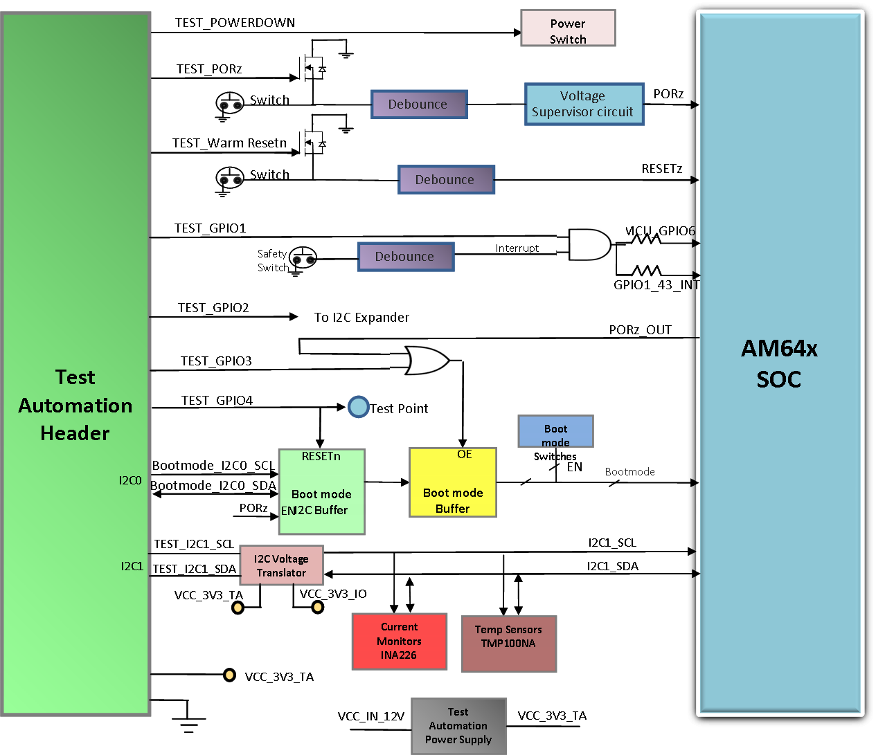
A Test automation header J38 is provided to allow an external controller to control the power on/off, boot modes, reset functionality and current measurement to support automated testing. The test automation header includes four GPIOs, two I2C interfaces. The basic controls as shown in Table 3-16.
| Signal | Signal Type | Function |
|---|---|---|
| POWER_DOWN | GPIO | Instructs the EVM to power down all circuits |
| POR | GPIO | Creates a PORz into the AM64x SoC |
| WARM_RESET | GPIO | Creates a RESETz into the AM64x SoC |
| GPIO1 | GPIO | GPIO for communication with AM64x SoC |
| GPIO2 | GPIO | Connected to I2C IO Expander |
| GPIO3 | GPIO | Used to Enable the BOOTMODE Buffer |
| GPIO4 | GPIO | Used to Reset the Boot mode IO Expander |
| I2C0 | I2C | Communicates with Boot mode I2C buffer |
| I2C2 | I2C | Communicates with INA226 current measurement devices |
One of the I2C interface from Test automation header is connected to an I2C IO expander, which can drive the Boot mode pins of the processor.
The other I2C interface is connected to the current measurement and temperature sensing devices present on the I2C1 port of the SoC.
The Test Automation connector is used by Texas Instruments for control of software regression testing and comparative power measurements. The connector is provided to allow customers to develop their own testing and power measurements of customer applications.
Power measurements varies based on silicon process and environment and measurements can only used for comparison with other measurements taken on the same EVM.
 Figure 3-12 Test Automation Header
| Pin No. | Signal | IO Direction (to CP board) |
|---|---|---|
| 1 | VCC3V3_1 | Power (out) |
| 2 | VCC3V3_1 | Power (out) |
| 3 | VCC3V3_1 | Power (out) |
| 4 | NC | NA |
| 5 | NC | NA |
| 6 | NC | NA |
| 7 | DGND | Ground |
| 8 | NC | NA |
| 9 | NC | NA |
| 10 | NC | NA |
| 11 | NC | NA |
| 12 | NC | NA |
| 13 | NC | NA |
| 14 | NC | NA |
| 15 | NC | NA |
| 16 | DGND | Ground |
| 17 | NC | NA |
| 18 | NC | NA |
| 19 | NC | NA |
| 20 | NC | NA |
| 21 | NC | NA |
| 22 | NC | NA |
| 23 | NC | NA |
| 24 | NC | NA |
| 25 | DGND | Ground |
| 26 | TEST_POWERDOWN | Input |
| 27 | TEST_PORz | Input |
| 28 | TEST_WARMRESETn | Input |
| 29 | NC | NA |
| 30 | TEST_GPIO1 | Bidirectional |
| 31 | TEST_GPIO2 | Bidirectional |
| 32 | TEST_GPIO3 | Input |
| 33 | TEST_GPIO4 | Input |
| 34 | DGND | Ground |
| 35 | NC | NA |
| 36 | SOC_I2C1_SCL | Bidirectional |
| 37 | BOOTMODE_I2C_SCL | Bidirectional |
| 38 | SOC_I2C1_SDA | Bidirectional |
| 39 | BOOTMODE_I2C_SDA | Bidirectional |
| 40 | DGND | Ground |
| 41 | DGND | Ground |
| 42 | DGND | Ground |