SPRUJ63A September 2022 – October 2023
- 1
- Trademarks
- 1Introduction
- 2Important Usage Notes
-
3System Description
- 3.1 Key Features
- 3.2 Functional Block Diagram
- 3.3 Power-On/Off Procedures
- 3.4
Peripheral and Major Component
Description
- 3.4.1 Clocking
- 3.4.2 Reset
- 3.4.3 Power
- 3.4.4 Configuration
- 3.4.5 JTAG
- 3.4.6 Test Automation
- 3.4.7 UART Interfaces
- 3.4.8 Memory Interfaces
- 3.4.9 Ethernet Interface
- 3.4.10 Display Interface
- 3.4.11 USB 2.0 Interface
- 3.4.12 PCIe Interface
- 3.4.13 High Speed Expansion Interface
- 3.4.14 CAN Interface
- 3.4.15 Interrupt
- 3.4.16 ADC Interface
- 3.4.17 Safety Connector
- 3.4.18 SPI Interfaces
- 3.4.19 I2C Interfaces
- 3.4.20 FSI Interface
- 4Known Issues and Modifications
- 5References
- 6Revision History
3.4.3.6 AM64x/AM243x Power
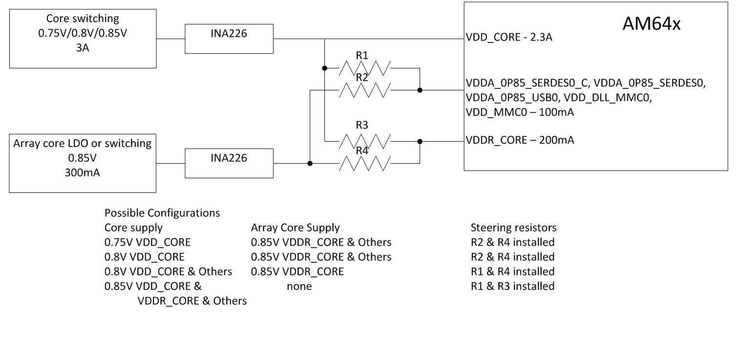
The Core voltage of the AM64x/AM243x can be powered by 0.75 V or 0.8 V or 0.85 V based on the power optimization requirement. TI recommends to use a single voltage source when the SoC Core voltage (VDD_CORE) and SoC Array Core Voltage (VDDR_CORE) and other array core voltages (VDDA_0P85_SERDES0_C, VDDA_0P85_SERDES0, VDDA_0P85_USB0, VDD_DLL_MMC0, VDD_MMC0) is 0.85 V. In cases where the SoC Core voltage is required to be 0.75 V or 0.8 V and SoC Array Core Voltage and other Array Core voltages is required to be 0.85 V, there needs to be separate voltage supply for the SoC Core voltage and an separate supply for the SoC Array Core voltages.
This EVM has a provision for providing single voltage supply or different voltage supply to the SoC Core and SoC Array Core and other Array Core Voltages and based requirement. This can be configured by the placement of resistors as mentioned in Figure 3-8.
 Figure 3-8 AM64x/AM243x Core Supply and Array Core Supply Options
- PROC101x-001 BOM variant, implements the AM6442 and requires 0.75 V supplied to the VDD_CORE and 0.85 V supplied to VDDR_CORE. In this variant R2 and R4 are installed by default and VDD_CORE supply (U25) is setup for 0.75 V operation.
- PROC101x-002 BOM variant, implements the AM2434 and requires 0.85 V supplied to VDD_CORE and VDDR_CORE. In this variant R1 and R3 are installed by default and VDD_CORE supply (U25) is setup for 0.85 V operation.
The SoC has different IO groups. Each IO group is powered by specific power supplies as shown in Table 3-6.
| SI.No. | Power Supply | SoC Supply Rails | IO Power Group | Power |
|---|---|---|---|---|
| 1 | VDDA_CORE | VDDA_0P85_SERDES0 | SERDES0 | 0.85 |
| VDDA_0P85_SERDES0_C | 0.85 | |||
| VDDA_0P85_USB0 | USB0 | 0.85 | ||
| VDD_MMC0 | MMC0 | 0.85 | ||
| 2 | SoC_DVDD3V3 | VDDS_MCU | MCU | 3.3 |
| VDDA_3P3_USB0 | USB0 | 3.3 | ||
| VDDSHV0 | General | 3.3 | ||
| VDDSHV1 | PRG0 | 3.3 | ||
| VDDSHV2 | PRG1 | 3.3 | ||
| VDDSHV3 | GPMC | 3.3 | ||
| 3 | VDDA_1V8_MCU | VDDA_MCU | MCU | 1.8 |
| 4 | VDDA_MCU_ADC | VDDA_ADC | ADC0 | 1.8 |
| 5 | VDDA_1V8_SERDES | VDDA_1P8_SERDES0 | SERDES0 | 1.8 |
| 6 | VDDA_1V8_USB0 | VDDA_1P8_USB0 | USB0 | 1.8 |
| 7 | VDDA_1V8 | VDDS_OSC | OSC0 | 1.8 |
| VDDA_TEMP_0/1 | 1.8 | |||
| VDDA_PLL_0/1/2 | 1.8 | |||
| 8 | VDD_DDR4 | VDDS_DDR | DDR0 | 1.2 |
| VDDS_DDR_C | 1.2 | |||
| 9 | SOC_DVDD1V8 | VDDSHV4 | FLASH | 1.8 |
| VDDS_MMC0 | MMC0 | 1.8 | ||
| 10 | VDDSHV_SD_IO | VDDSHV5 | MMC1 | 1.8 |