SPRUJ63A September 2022 – October 2023
- 1
- Trademarks
- 1Introduction
- 2Important Usage Notes
-
3System Description
- 3.1 Key Features
- 3.2 Functional Block Diagram
- 3.3 Power-On/Off Procedures
- 3.4
Peripheral and Major Component
Description
- 3.4.1 Clocking
- 3.4.2 Reset
- 3.4.3 Power
- 3.4.4 Configuration
- 3.4.5 JTAG
- 3.4.6 Test Automation
- 3.4.7 UART Interfaces
- 3.4.8 Memory Interfaces
- 3.4.9 Ethernet Interface
- 3.4.10 Display Interface
- 3.4.11 USB 2.0 Interface
- 3.4.12 PCIe Interface
- 3.4.13 High Speed Expansion Interface
- 3.4.14 CAN Interface
- 3.4.15 Interrupt
- 3.4.16 ADC Interface
- 3.4.17 Safety Connector
- 3.4.18 SPI Interfaces
- 3.4.19 I2C Interfaces
- 3.4.20 FSI Interface
- 4Known Issues and Modifications
- 5References
- 6Revision History
3.4.8.3 OSPI Interface
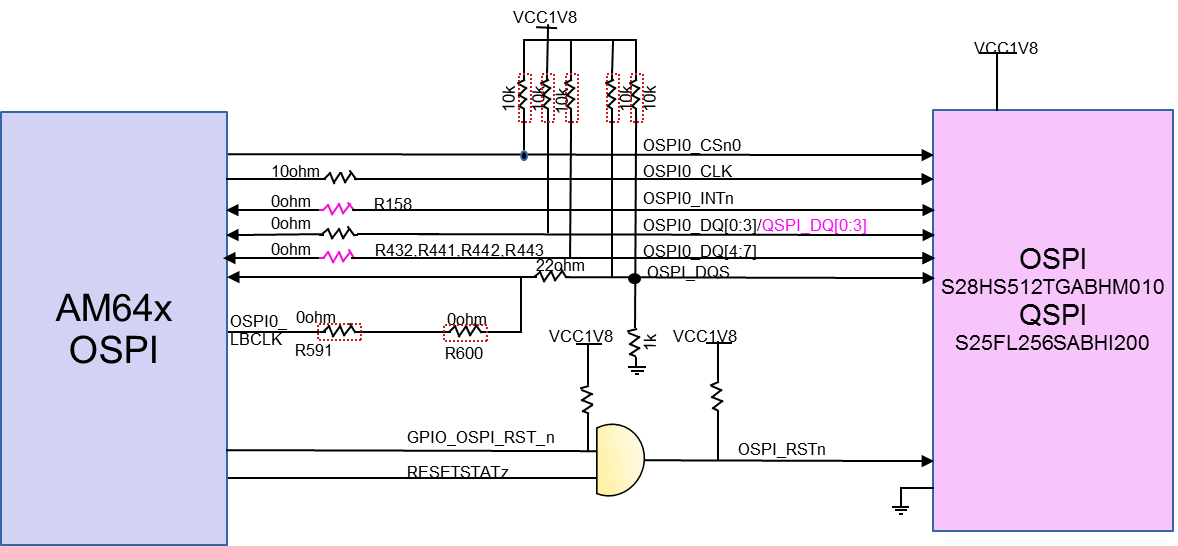
The EVM has 512 Mbit OSPI memory device of part number S28HS512TGABHM010 from Cypress is connected to OSPI0 interface of AM64x/AM243x SoC. The OSPI supports single and double data rates with memory speed up to 200MBps SDR and 400MBps DDR (200 MHz clock speed).
Two signals are routed to OSPI0_DQS:
- OSPI0_DQS from the memory device.
- OSPI0_LBCLK from SoC.
To route DQS from memory device, Mount R601 and R592 and DNI R600 and R591.
To route OSPI0_LBCLK from SoC, Mount R600 and R591 and DNI R601 and R592
OSPI and QSPI implementation: 0 Ω resistors are provided for DATA[7:0], DQS, INT# and CLK signals. Footprints to mount external pull up resistors are provided on DATA[7:0] to prevent bus floating. The footprint for the OSPI memory also allows the installation of either a QSPI memory or an OSPI memory. S25FL256SABHI200 from Cypress is used in variants where QSPI flash is required. The 0 ohm resistors used in pins OSPI_DATA[4:7] are removed if QSPI flash is mounted.
Remove 0E resistors from the following
- OSPI_DQ4 to OSPI_DQ7 nets (R432, R441, R442, R443).
- OSPI_INTn (R158).
 Figure 3-17 AM64x/AM243x OSPI Interface