SWRA720 February 2022 CC1352P , CC1352P7 , CC1352R , CC1354P10 , CC1354R10 , CC2640R2F , CC2640R2F-Q1 , CC2640R2L , CC2642R , CC2642R-Q1 , CC2651P3 , CC2651R3 , CC2651R3SIPA , CC2652P , CC2652P7 , CC2652PSIP , CC2652R , CC2652R7 , CC2652RB , CC2652RSIP , CC2674P10 , CC2674R10
4 Setting up the hardware
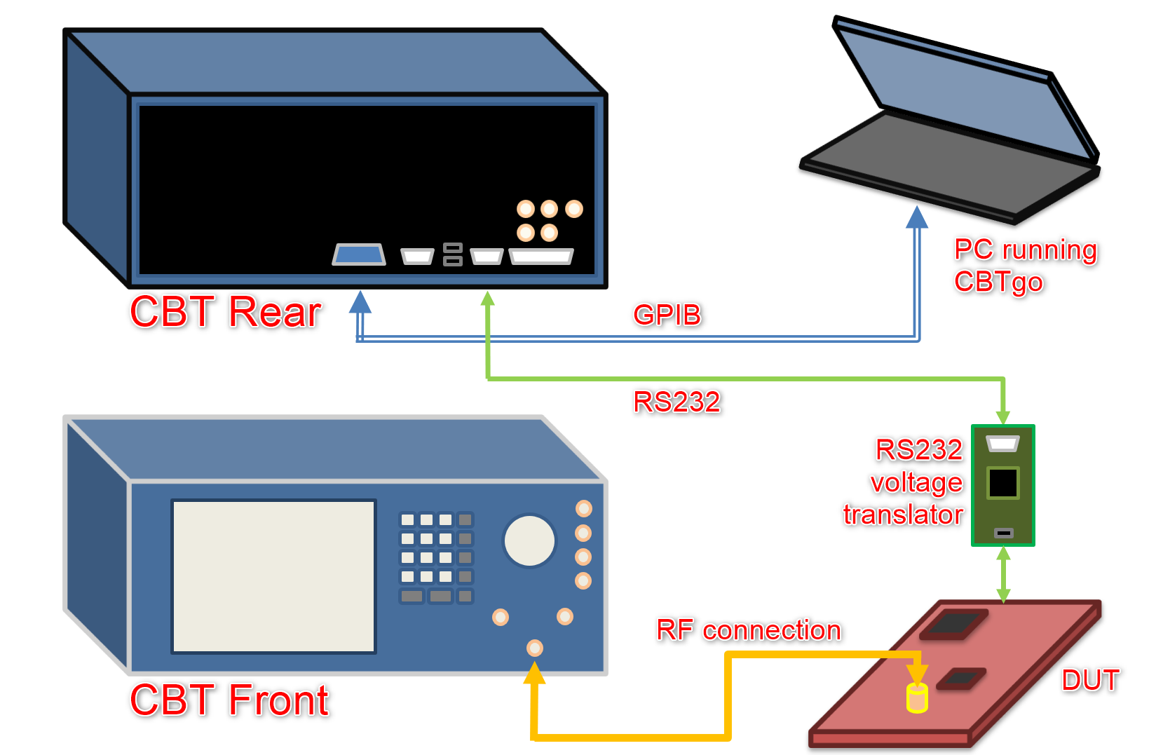
The overall setup to perform Bluetooth Low Energy using the CBT Bluetooth tester is shown in Figure 4-1
 Figure 4-1 The test setup
-
First step is to install the CBTgo software in your host PC. Check the Requirements section for download locations.
-
The CBTgo Help (F1 key) is very helpful to understand the setup and connections required. Check the topics Quick Start → Connecting the PD to the R&S CBT and Quick Start → Connecting Bluetooth Low Energy Device
-
-
Connect the GPIB interface of the CBT unit to the GPIB interface of the host PC. This procedure will not get into the details about how to configure the GPIB interface in your host PC.
-
Connect the RS232 voltage translator to the port on the back of the CBT unit.
-
The CBT RS232 port pinout corresponds to a DTE (Data Terminal Equipment) - i.e., pin 2 is Rx, pin 3 is Tx and pin 5 is GND.
-
Most RS232 voltage translators expect to be connected to a DTE, so use a straight serial cable (not null modem) - check the documentation of your RS232 voltage translator unit.
-
-
Connect the output of the RS232 voltage translator to the DUT.
-
Be sure to connect the Tx output of the voltage translator to the Rx input of the DUT. Similarly, connect the Rx input of the voltage translator to the Tx output of the DUT.
-
Connect the GND pin of the voltage translator to the GND pin of the DUT.
CAUTION: Be extremely careful with ground voltage differences that can damage the tester, the host PC or the DUT (for additional details, check this video) -
-
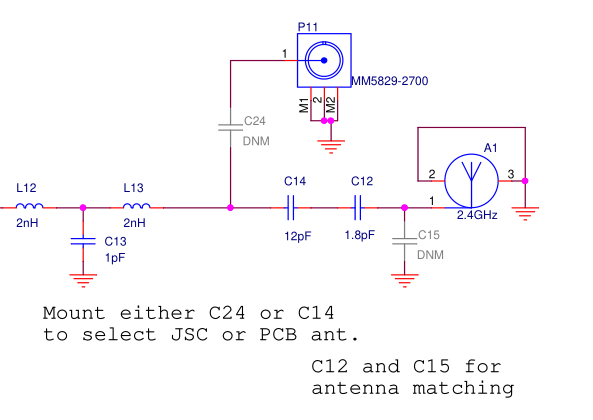
Perform the RF connection between the CBT and the DUT. On the Launchpad, a circuit modification is required to divert the RF path from the stripline antenna to the JSC connector mounted on the board.
The Launchpad design files (available for download as a .ZIP package on the product page at https://www.ti.com) has complete schematics and contains instructions to divert the RF path, as shown in Figure 4-2 for the LAUNCHXL-CC26X2R1:
 Figure 4-2 The schematic example
-
Any RF connections must be thoroughly characterized using a VNA or a calibrated Spectrum Analyzer, as differences in attenuation across the spectrum range may cause tests to fail or show inaccurate results.
-
An external attenuator will likely be needed.
-
-
Power on the system in this order: host PC, CBT, DUT and RS232 voltage translator.
-
It was observed that powering the RS232 voltage translator before the DUT can cause it to be in an unstable state.
-
-
The DUT must have a DTM software loaded and running on it, so it can properly receive the HCI commands from the CBT unit.
-
If the DUT maps the pins of the UART port the same way as our Launchpads, the host_test project from our SDKs can be used.
-
Attention must be taken also if there are no variations with regards to the crystal and other hardware aspects that influence the RF configuration.
-