TIDT319 December   2022


  1.   Description
  2.   Features
  3.   Applications
  4. 1Test Prerequisites
    1. 1.1 Voltage and Current Requirements
    2. 1.2 Considerations
    3. 1.3 Dimensions
  5. 2Testing and Results
    1. 2.1 Efficiency Graph
    2. 2.2 Loss Graph
    3. 2.3 Load Regulation
    4. 2.4 Thermal Images
      1. 2.4.1 Summary, Hottest Spot High-Side FET Q6, NVMFS5C645NL
      2. 2.4.2 Thermal Images
      3. 2.4.3 Thermal Mechanics
    5. 2.5 Bode Plots
      1. 2.5.1 Bode Plot Summary, Loop Bandwidth 16 kHz
      2. 2.5.2 24-V Input Voltage
      3. 2.5.3 36-V Input Voltage
      4. 2.5.4 48-V Input Voltage
  6. 3Waveforms for 2 × LM5143A-Q1 in Four Phase Configuration and Interleaved Operation
    1. 3.1 Switching
      1. 3.1.1 Overview of the Four Switching Phases
        1. 3.1.1.1 24-V Input Voltage
        2. 3.1.1.2 36-V Input Voltage
        3. 3.1.1.3 48-V Input Voltage
      2. 3.1.2 Low-Side FET
        1. 3.1.2.1 Switch Node to GND
        2. 3.1.2.2 Low-Side FET Gate to GND
      3. 3.1.3 High-Side FET
        1. 3.1.3.1 Switch Node to VIN
        2. 3.1.3.2 High-Side FET Gate to Switch Node
    2. 3.2 Output Voltage Ripple
    3. 3.3 Input Voltage Ripple
      1. 3.3.1 Board Input
        1. 3.3.1.1 24-V Input Voltage
        2. 3.3.1.2 36-V Input Voltage
        3. 3.3.1.3 48-V Input Voltage
      2. 3.3.2 Power Stage Input, No Input Filter
        1. 3.3.2.1 24-V Input Voltage
        2. 3.3.2.2 36-V Input Voltage
        3. 3.3.2.3 48-V Input Voltage
    4. 3.4 Load Transients
      1. 3.4.1 Load Transient 10 A to 50 A (80 %)
      2. 3.4.2 Load Transient 5 A to 50 A (90 %)
    5. 3.5 Start-Up Sequence
    6. 3.6 Shutdown Sequence
  7.   A Individual Adjusting of the Rising Edge and Falling Edge With LM5143A
    1.     A.1 2.21-Ω High and 4.75-Ω Low Resistor in Before Gate of the High-Side FET
    2.     A.2 2 × 4.75-Ω Resistors in Before Gate of the High-Side FET
  8.   B Measurements Across the Low-Side FETs to Check at All Four Phases
    1.     B.1 FET Q3
    2.     B.2 FET Q4
    3.     B.3 FET Q7
    4.     B.4 FET Q8
  9.   C ON Demand – Assembly of Thermal Interface
    1.     C.1 Thermal Interface Example

ON Demand – Assembly of Thermal Interface

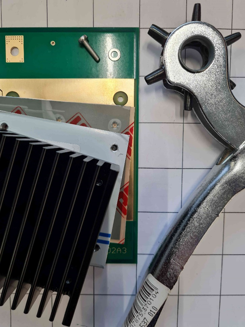
GUID-20221026-SS0I-S055-79BC-QHWPVLPM0LNZ-low.png Figure C-1 Stack: PCB – Thermal Foil – Adapter - Heat Sink
  • Drill the nine holes (diameter 3.5 mm) to Aluminum adapter
    150 mm × 75 mm × 5 mm; for correct dimensions use the Altium Designer® file.
  • Drill another nine holes (diameter 2.5 mm) to heat sink and cut threads M3
  • Add nine holes (diameter 3 mm) to the thermal foil using a punch pliers; so far this is the best choice.
  • Attention: Less adhesive side of thermal foil (RS) shows towards adapter, strong adhesive side (3M) shows towards the PCB.
  • Remove protection foil on less adhesive side only,
    keep protection foil on the other side. Now place the foil at the aluminum adapter.
  • Place just the nine screws plus washers at the PCB and place the top down on the PCB, two pieces of tape keep the screws in place, so there are nine bolts on the other side, this helps for the next step.
  • Remove protection foil at the strong adhesive side of the thermal foil, remove white protection foil at the adapter and place the adapter precisely on PCB.
  • Flip by keeping the adapter in place and set the adapter and PCB on top of heat sink, remove tapes and fix the screws. This completes the process

EMI: the adapter and heat sink are floating and provide the shortest connection J3 GND to the screw left of the L2 heat sink. Figure C-2 shows a GND connection.
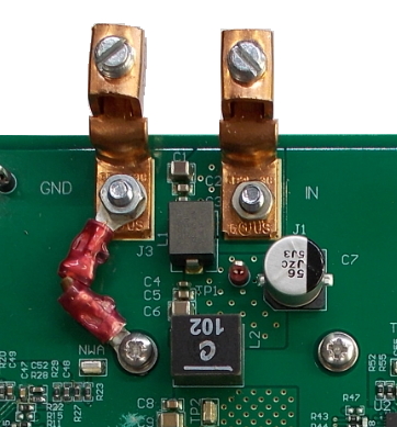
GUID-20221110-SS0I-2HF6-8MJX-XBPL6L29L7VS-low.jpg Figure C-2 GND Connection