TIDT319 December   2022


  1.   Description
  2.   Features
  3.   Applications
  4. 1Test Prerequisites
    1. 1.1 Voltage and Current Requirements
    2. 1.2 Considerations
    3. 1.3 Dimensions
  5. 2Testing and Results
    1. 2.1 Efficiency Graph
    2. 2.2 Loss Graph
    3. 2.3 Load Regulation
    4. 2.4 Thermal Images
      1. 2.4.1 Summary, Hottest Spot High-Side FET Q6, NVMFS5C645NL
      2. 2.4.2 Thermal Images
      3. 2.4.3 Thermal Mechanics
    5. 2.5 Bode Plots
      1. 2.5.1 Bode Plot Summary, Loop Bandwidth 16 kHz
      2. 2.5.2 24-V Input Voltage
      3. 2.5.3 36-V Input Voltage
      4. 2.5.4 48-V Input Voltage
  6. 3Waveforms for 2 × LM5143A-Q1 in Four Phase Configuration and Interleaved Operation
    1. 3.1 Switching
      1. 3.1.1 Overview of the Four Switching Phases
        1. 3.1.1.1 24-V Input Voltage
        2. 3.1.1.2 36-V Input Voltage
        3. 3.1.1.3 48-V Input Voltage
      2. 3.1.2 Low-Side FET
        1. 3.1.2.1 Switch Node to GND
        2. 3.1.2.2 Low-Side FET Gate to GND
      3. 3.1.3 High-Side FET
        1. 3.1.3.1 Switch Node to VIN
        2. 3.1.3.2 High-Side FET Gate to Switch Node
    2. 3.2 Output Voltage Ripple
    3. 3.3 Input Voltage Ripple
      1. 3.3.1 Board Input
        1. 3.3.1.1 24-V Input Voltage
        2. 3.3.1.2 36-V Input Voltage
        3. 3.3.1.3 48-V Input Voltage
      2. 3.3.2 Power Stage Input, No Input Filter
        1. 3.3.2.1 24-V Input Voltage
        2. 3.3.2.2 36-V Input Voltage
        3. 3.3.2.3 48-V Input Voltage
    4. 3.4 Load Transients
      1. 3.4.1 Load Transient 10 A to 50 A (80 %)
      2. 3.4.2 Load Transient 5 A to 50 A (90 %)
    5. 3.5 Start-Up Sequence
    6. 3.6 Shutdown Sequence
  7.   A Individual Adjusting of the Rising Edge and Falling Edge With LM5143A
    1.     A.1 2.21-Ω High and 4.75-Ω Low Resistor in Before Gate of the High-Side FET
    2.     A.2 2 × 4.75-Ω Resistors in Before Gate of the High-Side FET
  8.   B Measurements Across the Low-Side FETs to Check at All Four Phases
    1.     B.1 FET Q3
    2.     B.2 FET Q4
    3.     B.3 FET Q7
    4.     B.4 FET Q8
  9.   C ON Demand – Assembly of Thermal Interface
    1.     C.1 Thermal Interface Example

24-V Input Voltage

GUID-20221208-SS0I-6HXS-X3RZ-FQJ7S96PZWWC-low.jpg

(SW1 to SW4)

20 V / div

2 µs / div

Full bandwidth

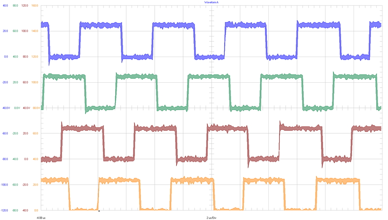
Figure 3-1 Four Switching Phases at 0, 90, 180, 270 Degrees Phase Shift at 24 VIN
Primary Controller U1 phase 1(1) 0 degrees
phase 2(1) 180 degrees
Secondary Controller U2 phase 3(1) 90 degrees
phase 4(1) 270 degrees
The background color in the table cells correspond to the waveform colors in Figure 3-1.

Figure 3-1 highlights the four phase interleaved operation of the two stacked controllers in primary and secondary configuration. Four phase interleaved operation results in ripple rejection at 25%, 50% and 75% duty cycle.

This evidence shows that at 24-V input voltage (duty cycle around 50%) and at 480-V input voltage (duty-cycle around 25%) and around 12-V output voltage, the ripple rejection is best.

This ripple rejection is illustrated in Figure 3-8, output ripple < 10 mVPP and noise < 50 mVPP.