TIDT319 December   2022


  1.   Description
  2.   Features
  3.   Applications
  4. 1Test Prerequisites
    1. 1.1 Voltage and Current Requirements
    2. 1.2 Considerations
    3. 1.3 Dimensions
  5. 2Testing and Results
    1. 2.1 Efficiency Graph
    2. 2.2 Loss Graph
    3. 2.3 Load Regulation
    4. 2.4 Thermal Images
      1. 2.4.1 Summary, Hottest Spot High-Side FET Q6, NVMFS5C645NL
      2. 2.4.2 Thermal Images
      3. 2.4.3 Thermal Mechanics
    5. 2.5 Bode Plots
      1. 2.5.1 Bode Plot Summary, Loop Bandwidth 16 kHz
      2. 2.5.2 24-V Input Voltage
      3. 2.5.3 36-V Input Voltage
      4. 2.5.4 48-V Input Voltage
  6. 3Waveforms for 2 × LM5143A-Q1 in Four Phase Configuration and Interleaved Operation
    1. 3.1 Switching
      1. 3.1.1 Overview of the Four Switching Phases
        1. 3.1.1.1 24-V Input Voltage
        2. 3.1.1.2 36-V Input Voltage
        3. 3.1.1.3 48-V Input Voltage
      2. 3.1.2 Low-Side FET
        1. 3.1.2.1 Switch Node to GND
        2. 3.1.2.2 Low-Side FET Gate to GND
      3. 3.1.3 High-Side FET
        1. 3.1.3.1 Switch Node to VIN
        2. 3.1.3.2 High-Side FET Gate to Switch Node
    2. 3.2 Output Voltage Ripple
    3. 3.3 Input Voltage Ripple
      1. 3.3.1 Board Input
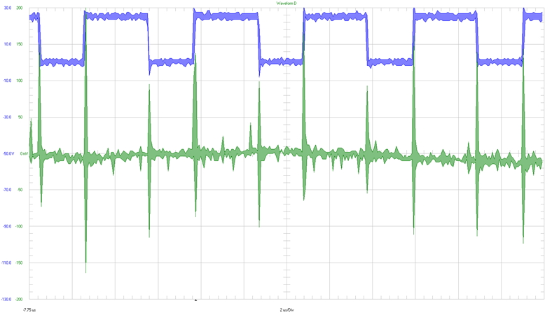
        1. 3.3.1.1 24-V Input Voltage
        2. 3.3.1.2 36-V Input Voltage
        3. 3.3.1.3 48-V Input Voltage
      2. 3.3.2 Power Stage Input, No Input Filter
        1. 3.3.2.1 24-V Input Voltage
        2. 3.3.2.2 36-V Input Voltage
        3. 3.3.2.3 48-V Input Voltage
    4. 3.4 Load Transients
      1. 3.4.1 Load Transient 10 A to 50 A (80 %)
      2. 3.4.2 Load Transient 5 A to 50 A (90 %)
    5. 3.5 Start-Up Sequence
    6. 3.6 Shutdown Sequence
  7.   A Individual Adjusting of the Rising Edge and Falling Edge With LM5143A
    1.     A.1 2.21-Ω High and 4.75-Ω Low Resistor in Before Gate of the High-Side FET
    2.     A.2 2 × 4.75-Ω Resistors in Before Gate of the High-Side FET
  8.   B Measurements Across the Low-Side FETs to Check at All Four Phases
    1.     B.1 FET Q3
    2.     B.2 FET Q4
    3.     B.3 FET Q7
    4.     B.4 FET Q8
  9.   C ON Demand – Assembly of Thermal Interface
    1.     C.1 Thermal Interface Example

24-V Input Voltage

GUID-20221209-SS0I-6C0F-DL3H-WNPQDXB41XF4-low.jpg

SW2 ⇒ 20 V / div


VIN ⇒ 50 mV / div


2 µs / div

Full bandwidth

Figure 3-9 Voltage Ripple: Board Input (AC Coupled) at 24-V Input Voltage