TIDT328 april   2023


  1.   1
  2.   Description
  3.   Features
  4.   Applications
  5. 1Test Prerequisites
    1. 1.1 Voltage and Current Requirements
    2. 1.2 Considerations
    3. 1.3 Dimensions
  6. 2Testing and Results
    1. 2.1 Efficiency Graphs
    2. 2.2 Load Regulation
    3. 2.3 Thermal Images
      1. 2.3.1 Unmodulated 60 VDC - Output
      2. 2.3.2 60 VAC - Output Modulated With 120-Hz Sinus (0 V – 5 V)
      3. 2.3.3 Conclusion
    4. 2.4 Bode Plot at Maximum Duty Cycle
  7. 3Waveforms
    1. 3.1 Switching
      1. 3.1.1 Transistor Q1 Operating in Deep DCM
        1. 3.1.1.1 Drain to Source
        2. 3.1.1.2 Gate to Source
      2. 3.1.2 Diode D3 (Referenced to VOUT)
    2. 3.2 Output Voltage Ripple
    3. 3.3 Input Voltage Ripple
    4. 3.4 Start-Up Sequence
    5. 3.5 Shutdown Sequence
  8.   A Modulating the Output Voltage
    1.     A.1 Revision B
      1.      A.1.1 Bode Plot
      2.      A.1.2 Simulation
      3.      A.1.3 Measured Waveforms
        1.       A.1.3.1 Sinus 40 Hz
        2.       A.1.3.2 Sinus 100 Hz
        3.       A.1.3.3 Sawtooth 1
        4.       A.1.3.4 Sawtooth 2
        5.       A.1.3.5 Pure Triangle
        6.       A.1.3.6 Conclusion
    2.     A.2 Revision C
      1.      A.2.1 Bode Plot
      2.      A.2.2 Measured Waveforms
        1.       A.2.2.1 Sinus 120 Hz
        2.       A.2.2.2 Sawtooth 1
        3.       A.2.2.3 Sawtooth 2
        4.       A.2.2.4 Pure Triangle
      3.      A.2.3 Analysis Capacitor 1 µF, 100 V, X7R, 1206
        1.       A.2.3.1 DC-Bias
        2.       A.2.3.2 Resistance (ESR)
        3.       A.2.3.3 Reactance
        4.       A.2.3.4 Impedance

Sinus 120 Hz

GUID-20230314-SS0I-SPMR-6ZCQ-BLXSGDWXRKQ2-low.jpg

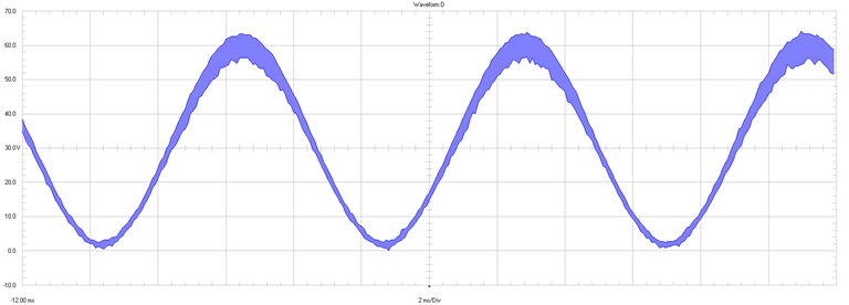
10 V / div

2 ms / div

full bandwidth

Figure 4-9 Modulation Sinusoidal (5 VPP + 2.5 V) 120 Hz, 12 VIN, 200-Ω Load

Modulation set to 120 Hz, sinusoidal output voltage looks promising, but the output ripple voltage is increased by lowering output impedance.


Ripple reduction – instead of using a single output capacitor 2.2 µF,100 V, X7R, 1210, a small improvement can be achieved by using several smaller capacitors in parallel ⇒ 3 × 1 µF, 100 V, X7R, 1206, that is, Murata GCJ31CR72A105KA01.