TIDT328 april   2023


  1.   1
  2.   Description
  3.   Features
  4.   Applications
  5. 1Test Prerequisites
    1. 1.1 Voltage and Current Requirements
    2. 1.2 Considerations
    3. 1.3 Dimensions
  6. 2Testing and Results
    1. 2.1 Efficiency Graphs
    2. 2.2 Load Regulation
    3. 2.3 Thermal Images
      1. 2.3.1 Unmodulated 60 VDC - Output
      2. 2.3.2 60 VAC - Output Modulated With 120-Hz Sinus (0 V – 5 V)
      3. 2.3.3 Conclusion
    4. 2.4 Bode Plot at Maximum Duty Cycle
  7. 3Waveforms
    1. 3.1 Switching
      1. 3.1.1 Transistor Q1 Operating in Deep DCM
        1. 3.1.1.1 Drain to Source
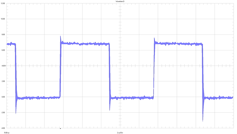
        2. 3.1.1.2 Gate to Source
      2. 3.1.2 Diode D3 (Referenced to VOUT)
    2. 3.2 Output Voltage Ripple
    3. 3.3 Input Voltage Ripple
    4. 3.4 Start-Up Sequence
    5. 3.5 Shutdown Sequence
  8.   A Modulating the Output Voltage
    1.     A.1 Revision B
      1.      A.1.1 Bode Plot
      2.      A.1.2 Simulation
      3.      A.1.3 Measured Waveforms
        1.       A.1.3.1 Sinus 40 Hz
        2.       A.1.3.2 Sinus 100 Hz
        3.       A.1.3.3 Sawtooth 1
        4.       A.1.3.4 Sawtooth 2
        5.       A.1.3.5 Pure Triangle
        6.       A.1.3.6 Conclusion
    2.     A.2 Revision C
      1.      A.2.1 Bode Plot
      2.      A.2.2 Measured Waveforms
        1.       A.2.2.1 Sinus 120 Hz
        2.       A.2.2.2 Sawtooth 1
        3.       A.2.2.3 Sawtooth 2
        4.       A.2.2.4 Pure Triangle
      3.      A.2.3 Analysis Capacitor 1 µF, 100 V, X7R, 1206
        1.       A.2.3.1 DC-Bias
        2.       A.2.3.2 Resistance (ESR)
        3.       A.2.3.3 Reactance
        4.       A.2.3.4 Impedance

Gate to Source

GUID-20230314-SS0I-FD9P-8W7W-QTDRLSNXT8SJ-low.jpg

2 V / div

2 µs / div

full bandwidth

GUID-20230314-SS0I-PDNC-N5MP-VZ59H80MLKB8-low.jpg
GUID-20230314-SS0I-Z9L9-NXLM-VVHR0SJHJZC4-low.jpg

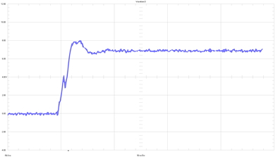
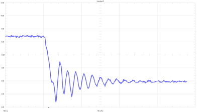
2 V / div

250 ns full scale

full bandwidth

Figure 3-2 Switching Q1 (Gate-Source)