TIDUF28 November 2023
- 1
- Description
- Resources
- Features
- Applications
- 6
- 1System Description
- 2System Overview
- 3System Design Theory
-
4Hardware, Software, Testing Requirements,
and Test Results
- 4.1 Hardware Requirements
- 4.2 Software Requirements
- 4.3 Test Setup
- 4.4 Test Results
- 5Design and Documentation Support
- 6About the Author
3.3 DC-Link (HV_BUS) Voltage Sensing
The TIDA-010255 is designed to operate at a nominal DC-link voltage of 320 VDC and a maximum DC-link voltage up to 400 VDC, corresponding to a single-phase 200-VAC to 250-VAC input. Accurate sensing of the DC-link voltage is important to calculate the corresponding duty cycle of the three-phase PWM, monitor for overvoltage and undervoltage, and estimate the amplitude of phase voltages.
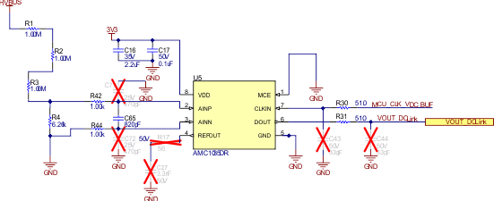
Due to the hot-side control architecture, the DC-link voltage can be sensed through a non-isolated delta-sigma modulator AMC1035 with a corresponding high-voltage resistor divider. The AMC1035 has a maximum bipolar input voltage range of ±1.25 V and a linear input voltage range of ±1 V. The high-impedance resistor dividers R1, R2, R3, and R4 are scaled to provide a 1-V signal at the AMC1035 input at 480-VDC bus voltage. R1, R2, and R3 are high-voltage resistors.
The AMC1035 analog input filter is designed similar to the AMC1306M05 in Section 3.2.2. However, the cutoff frequency is initially set to around 23-kHz. The analog input filter is determined by R4, R42, R44, and C65, and can be changed to any desired lower or higher cutoff frequency, for example in systems which monitor the AC voltage ripple on the DC-bus.
The MCE pin is set to low to configure for a bitstream data output at DOUT. Data at DOUT changes with the rising edge of the clock signal present on CLKIN. The line termination and filtering are similar as described in Section 3.2.3. A separate clock signal MCU_CLK_VDC_BUF is provided to allow the same of a different clock rate for DC-link voltage sensing, and is then configured for the three current-sensing modulators AMC1306M05. The AMC1035 supports clock input signals from 9 MHz to 21 MHz. The REFOUT is not used in this design and is terminated with C27 (3.3 nF) and a series resistor R17 (56 Ω).
 Figure 3-8 DC-link Voltage Sensing With Non-isolated Modulator Schematic