TIDUF28 November   2023


  1.   1
  2.   Description
  3.   Resources
  4.   Features
  5.   Applications
  6.   6
  7. 1System Description
    1. 1.1 Key System Specifications
  8. 2System Overview
    1. 2.1 Block Diagram
    2. 2.2 Highlighted Products
      1. 2.2.1 LMG3422R030
      2. 2.2.2 ISO7741
      3. 2.2.3 AMC1306M05
      4. 2.2.4 AMC1035
      5. 2.2.5 TPSM560R6H
      6. 2.2.6 TPSM82903
  9. 3System Design Theory
    1. 3.1 Power Switches
      1. 3.1.1 GaN-FET Selection Criterion
      2. 3.1.2 HVBUS Decoupling and 12-V Bootstrap Supply
      3. 3.1.3 GaN_FET Turn-on Slew Rate Configuration
      4. 3.1.4 PWM Input Filter and Dead-Time Calculation
      5. 3.1.5 Signal Level Shifting
      6. 3.1.6 LMG3422R030 Fault Reporting
      7. 3.1.7 LMG3422R030 Temperature Monitoring
    2. 3.2 Phase Current Sensing
      1. 3.2.1 Shunt
      2. 3.2.2 AMC1306M05 Analog Input-Filter
      3. 3.2.3 AMC1306M05 Digital Interface
      4. 3.2.4 AMC1306M05 Supply
    3. 3.3 DC-Link (HV_BUS) Voltage Sensing
    4. 3.4 Phase Voltage Sensing
    5. 3.5 Control Supply
    6. 3.6 MCU Interface
  10. 4Hardware, Software, Testing Requirements, and Test Results
    1. 4.1 Hardware Requirements
      1. 4.1.1 PCB
      2. 4.1.2 MCU Interface
    2. 4.2 Software Requirements
    3. 4.3 Test Setup
      1. 4.3.1 Precautions
      2. 4.3.2 Test Procedure
    4. 4.4 Test Results
      1. 4.4.1 24-V Input Control Supply
      2. 4.4.2 Propagation Delay PWM to Phase Voltage Switch Node
      3. 4.4.3 Switch Node Transient at 320-VDC Bus Voltage
      4. 4.4.4 Phase Voltage Linearity and Distortion at 320 VDC and 16-kHz PWM
      5. 4.4.5 Inverter Efficiency and Thermal Characteristic
        1. 4.4.5.1 Efficiency Measurements
        2. 4.4.5.2 Thermal Analysis and SOA Without Heat Sink at 320 VDC and 16-kHz PWM
  11. 5Design and Documentation Support
    1. 5.1 Design Files
      1. 5.1.1 Schematics
      2. 5.1.2 BOM
      3. 5.1.3 PCB Layout Recommendations
        1. 5.1.3.1 Layout Prints
      4. 5.1.4 Altium Project
      5. 5.1.5 Gerber Files
      6. 5.1.6 Assembly Drawings
    2. 5.2 Tools and Software
    3. 5.3 Documentation Support
    4. 5.4 Support Resources
    5. 5.5 Trademarks
  12. 6About the Author

PCB

The six GaN-FETs LMG3422R030 devices are mounted on top of the PCB, as well as the three phase current shunts and the high-voltage supply input connector J3, the 24-V input supply connector J5, the three-phase motor connector J4, and the connectors J6 to J9 and J11 to an external MCU, as well as J1 and J2 to interface to a F28379D C2000 MCU controlCARD.
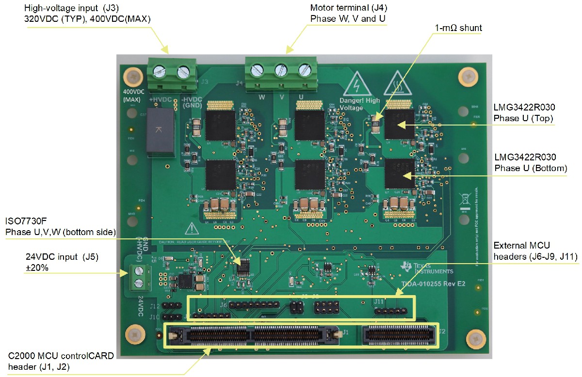
GUID-20231101-SS0I-4Z3M-85FQ-PMLWRTVKVPRS-low.jpg Figure 4-1 TIDA-010255 PCB Top View

The PCB bottom side shows the three isolated modulators AMC1306M25, the resistor dividers with the AMC1035 delta-sigma modulator for the DC-link voltage sensing and the six digital isolators ISO7741 for PWM level shifting. The 6 holes shown on the left and right allow for mounting a heat sink on the bottom-side of the PCB to connect to the six copper planes on the bottom-cooled LMG3422R030 GaN-FETs.
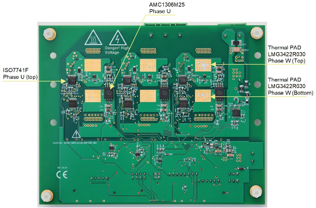
GUID-20231101-SS0I-L4KK-WRLK-Z0BFQFRRD9TJ-low.jpg Figure 4-2 TIDA-010255 PCB Bottom View