SLUSAQ9B December 2011 – December 2015 UC1875-SP
PRODUCTION DATA.
- 1 Features
- 2 Applications
- 3 Description
- 4 Revision History
- 5 Description (continued)
- 6 Pin Configuration and Functions
- 7 Specifications
- 8 Detailed Description
-
9 Application and Implementation
- 9.1 Application Information
- 9.2
Typical Application
- 9.2.1 Design Requirements
- 9.2.2
Detailed Design Procedure
- 9.2.2.1 Phase-Shifted Fundamentals
- 9.2.2.2 Circuit Schematic and Description
- 9.2.2.3 Initial Conditions (Time: t = t(0))
- 9.2.2.4 Right Leg Resonant Transition Interval (Time: t(0) < t < t(1))
- 9.2.2.5 Clamped Freewheeling Interval (Time: t(1) < t < t(2))
- 9.2.2.6 Left Leg Transition Interval (Time: t(2) < t < t(3))
- 9.2.2.7 Power Transfer Interval (Time: t(3) < t < t(4))
- 9.2.2.8 Switch Turn Off (Time: t(4))
- 9.2.2.9 Resonant Tank Considerations
- 9.2.2.10 Resonant Circuit Limitations
- 9.2.2.11 Stored Inductive Energy
- 9.2.2.12 Resonant Circuit Summary
- 9.2.2.13 Stored Energy Requirements
- 9.2.2.14 Minimum Primary Current
- 9.2.3 Application Curve
- 10Power Supply Recommendations
- 11Layout
- 12Device and Documentation Support
- 13Mechanical, Packaging, and Orderable Information
パッケージ・オプション
メカニカル・データ(パッケージ|ピン)
サーマルパッド・メカニカル・データ
発注情報
1 Features
- QML-V Qualified, SMD 5962-94555
- Rad-Tolerant: 50 kRad (Si) TID (1)
- Zero to 100% Duty Cycle Control
- Programmable Output Turn-On Delay
- Compatible with Voltage or Current Mode Topologies
- Practical Operation at Switching Frequencies to
1 MHz - Four 2-A Totem Pole Outputs
- 10-MHz Error Amplifier
- Undervoltage Lockout (UVLO)
- Low Startup Current – 150 µA
- Outputs Active Low During UVLO
- Soft-Start Control
- Latched Overcurrent Comparator With Full Cycle Restart
- Trimmed Reference
2 Applications
Power FPGAs
3 Description
The UC1875-SP implements control of a bridge power stage by phase-shifting the switching of one half-bridge with respect to the other, allowing constant frequency pulse-width modulation in combination with resonant, zero-voltage switching for high efficiency performance at high frequencies. This circuit may be configured to provide control in either voltage or current mode operation, with a separate overcurrent shutdown for fast fault protection.
A programmable time delay is provided to insert a dead-time at the turn-on of each output stage. This delay, providing time to allow the resonant switching action, is independently controllable for each output pair (A-B, C-D).
With the oscillator capable of operation at frequencies in excess of 2 MHz, overall switching frequencies to
1 MHz are practical. In addition to the standard free running mode, with the CLOCKSYNC pin, the user may configure these devices to accept an external clock synchronization signal, or may lock together up to 5 units with the operational frequency determined by the fastest device.
Device Information(1)
| PART NUMBER | PACKAGE | BODY SIZE (NOM) |
|---|---|---|
| UC1875-SP | LCCC (28) | 11.43 mm × 11.43 mm |
| CDIP (20) | 24.20 mm × 6.92 mm | |
| CFP (24) | 14.36 mm × 9.09 mm |
- For all available packages, see the orderable addendum at the end of the data sheet.
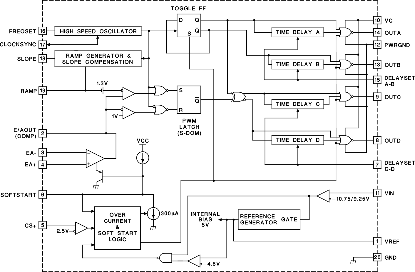
Block Diagram
