DLPU133 March 2024 DLPC964
- 1
- Abstract
- Trademarks
- 1Overview
-
2Apps FPGA
Modules
- 3.1 Apps FPGA Block Diagram
- 3.2 BPG Module
- 3.3 BRG Module
- 3.4 BRG_ST Module
- 3.5 PGEN Module
- 3.6 PGEN_MCTRL Module
- 3.7 PGEN_SCTRL Module
- 3.8 PGEN_PRM Module
- 3.9 PGEN_ADDR_ROM
- 3.10 HSSTOP Module
- 3.11 SSF Module
- 3.12 ENC Module
- 3.13 Xilinx IP
- 3.14 Reference Documents
- 3.15 DLPC964 Apps FPGA IO
- 3.16 Key Definitions
- 3Functional Configuration
-
4Appendix
- 5.1 Vivado Chipscope Captures
- 5.2 DLPC964 Apps Bitstream Loading
- 5.3
Interfacing To DLPC964 Controller with Aurora
64B/66B
- 5.3.1 Theory of Operation
- 5.3.2 Overview
- 5.3.3
Aurora 64B/66B TX Core and RTL Generation
- 5.3.3.1 Select Aurora 64B66B From IP Catalog
- 5.3.3.2 Configure Core Options
- 5.3.3.3 Lane Configurations
- 5.3.3.4 Shared Logic Options
- 5.3.3.5 Generate Example Design Files
- 5.3.3.6 RTL File List
- 5.3.3.7 Single Channel 3 Lanes Aurora Core RTL Wrapper
- 5.3.3.8 Four Channels 12 Lanes Top Level RTL Wrapper
- 5.3.3.9 Block Start with Block Control Word
- 5.3.3.10 Block Complete with DMDLOAD_REQ
- 5.3.3.11 DMDLOAD_REQ Setup Time Requirement
- 5.3.3.12 Single Channel Transfer Mode
- 5.3.3.13 DMD Block Array Data Mapping
- 5.3.3.14 Xilinx IBERT
- 5Abbreviations and Acronyms
- 6Related Documentation from Texas Instruments
4.3.3.10 Block Complete with DMDLOAD_REQ
Refer to Figure 4-11: DLPC964 System Block Diagram
DMDLOAD_REQ is an output signal from the Apps FPGA to DLPC964 Controller.
Once an Aurora block data transfer is completed, the Apps FPGA user logics must assert the DMDLOAD_REQ to signal the DLPC964 that this is the end of a DMD block and trigger to carry out the operation encoded in the Block Control word.
Guidelines for asserting the DMDLOAD_REQ signal and sending Block Control word:
- Apps FPGA user logics must wait
for the block transfer to be completed on all four Aurora data channels before
asserting DMDLOAD_REQ.
- Apps FPGA must take into account that the four Aurora data channel interfaces are not fully synchronous to each other, thus data completion do not happen at the exact same clock cycle. Therefore, the Apps FPGA must monitor and verify the Aurora block data transfer is completed on all four channels before asserting DMDLOAD_REQ.
Note: Asserting DMDLOAD_REQ before completion of Aurora block transfer can result in data not loaded properly to DMD. - DMDLOAD_REQ can be asserted immediately after completing an Aurora block transfer, as long as the 300ns DMDLOAD_REQ setup time is met (refer to Section 4.3.3.11 for more information).
- Apps FPGA user logics must assert DMDLOAD_REQ for the current block before initiate the transmission of the next new DMD block. Every block must start with a Block Control word packet and end with DMDLOAD_REQ assertion.
- DMDLOAD_REQ is still required for operations that do not involve block data transfer (such as block clear/set operation), and must still meet the 300ns setup time (refer to Section 4.3.3.11 for more information).
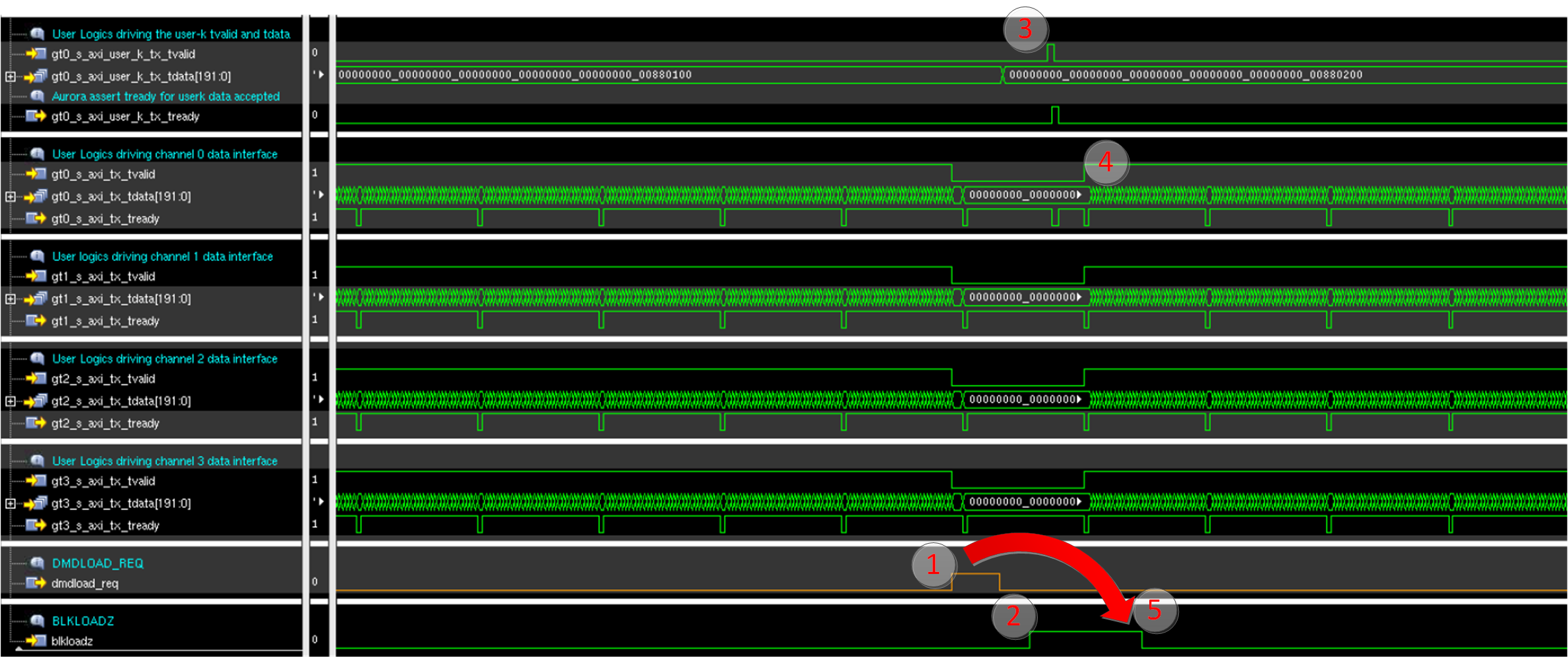
- Refer to Figure 4-19 for the scenario where after the Apps user
logics has completed the transfer of current block. The user can find that the
DLPC964 is still loading the previous block to the DMD (for example, BLKLOADZ is
low). The Apps FPGA can still assert the DMDLOAD_REQ while BLKLOADZ is low
because the DLPC964 can detect and store this DMDLOAD_REQ request. After
completing the Aurora data transfer of the current DMD block and asserting the
DMDLOAD_REQ signal, the Apps FPGA must wait for the de-assertion of BLKLOADZ by
the DLPC964 (for example, BLKLOADZ transition from low to high) before starting
the next block. De-assertion of BLKLOADZ means the DLPC964 has completed the DMD
data loading operation for previous block and a data buffer is freed up for
accepting a new data block from the Aurora interface. Note: The DLPC964 has two data block buffers; one for receiving the incoming Aurora data block, the other for holding the previous block for streaming out to DMD. The buffers can be overrun and data is not loaded correctly to the DMD if Apps FPGA does not synchronize the Aurora block transfer with the BLKLOADZ’s de-assertion signal.
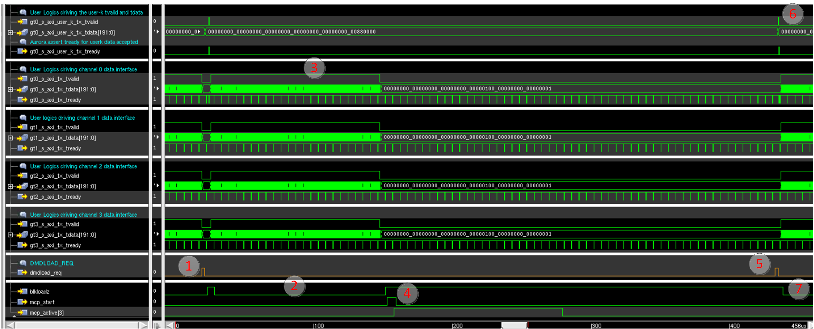
- Refer to Figure 4-20 for a scenario where the Apps FPGA chooses to send the DLPC964 a DMD data block, but delay the assertion of the DMDLOAD_REQ.
 Figure 4-19 End of Block DMDLOAD_REQ
Assertion Follow By New Block Control Word Waveform
Figure 4-19 End of Block DMDLOAD_REQ
Assertion Follow By New Block Control Word Waveform- Apps FPGA user logics assert DMDLOAD_REQ immediately after the completion of current block data transmission on all four Aurora data interfaces.
- DLPC964 de-assert BLKLOADZ indicating completion of data loading operation for previous DMD block.
- Apps FPGA user logics detects the de-assertion of BLKLOADZ and send a new Block Control word on Aurora channel 0 user-k port for next block.
- Apps FPGA user logics sending data for the next block.
- BLKLOADZ asserted low by DLPC964 indicating that the data loading operation for the current block is triggered by DMDLOAD_REQ.
 Figure 4-20 DMDLOAD_REQ Delayed Assertion
Waveform
Figure 4-20 DMDLOAD_REQ Delayed Assertion
Waveform- Apps FPGA finishes sending the last block (block 15) data of current pattern and asserts DMDLOAD_REQ to instruct the DLPC964 to carry out the data load operation.
- DLPC964 loading data to block 15 triggered by DMDLOAD_REQ from 1.
- Apps FPGA sends the first block (block 0) of data of the next pattern over the Aurora data interfaces while the DLPC964 is loading block 15 of the current pattern.
- DLPC964 de-asserts BLKLOADZ after the data loading of block 15 of current pattern is complete. The Apps FPGA detected the BLKLOADZ de-assertion as the last block of the current pattern and has been loaded onto the DMD and issued a MCP_START for global block reset operation.
- The Apps FPGA delayed the assertion of DMDLOAD_REQ for block 0 for the next pattern due to the requirement of meeting the mirror settling time.
- Send Block Control word for block 1 for the next pattern after the assertion of DMDLOAD_REQ for block 0.
- DLPC964 asserts BLKLOADZ to indicate that the DMD data loading operation was triggered by DMDLOAD_REQ from part 5.