SBAS649B June 2021 – June 2022 DAC12DL3200
PRODUCTION DATA
- 1 Features
- 2 Applications
- 3 Description
- 4 Revision History
- 5 Pin Configuration and Functions
-
6 Specifications
- 6.1 Absolute Maximum Ratings
- 6.2 ESD Ratings
- 6.3 Recommended Operating Conditions
- 6.4 Thermal Information
- 6.5 Electrical Characteristics - DC Specifications
- 6.6 Electrical Characteristics - Power Consumption
- 6.7 Electrical Characteristics - AC Specifications
- 6.8 Timing Requirements
- 6.9 Switching Characteristics
- 6.10 Typical Characteristics
-
7 Detailed Description
- 7.1 Overview
- 7.2 Functional Block Diagram
- 7.3
Feature Description
- 7.3.1 DAC Output Modes
- 7.3.2 DAC Output Interface
- 7.3.3 LVDS Interface
- 7.3.4 Multi-Device Synchronization (SYSREF+/-)
- 7.3.5 Alarms
- 7.4 Device Functional Modes
- 7.5 Programming
- 8 Application and Implementation
- 9 Device and Documentation Support
- 10Mechanical, Packaging, and Orderable Information
3 Description
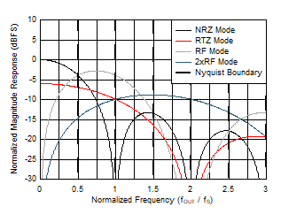
The DAC12DL3200 is a very low latency, dual channel, RF sampling digital-to-analog converter (DAC) capable of input and output rates of up to 3.2-GSPS in dual channel mode or 6.4-GSPS in single channel mode. The DAC can transmit signal bandwidths beyond 2 GHz at carrier frequencies approaching 8 GHz when using the multi-Nyquist output modes. The high output frequency range enables direct sampling through C-band (8 GHz) and beyond.
The DAC12DL3200 can be used as an I/Q baseband DAC in dual channel mode. The high sampling rate and output frequency range also makes the DAC12DL3200 capable of arbitrary waveform generation (AWG) and direct digital synthesis (DDS). An integrated DDS block enables single tone and two tone generation on chip.
The DAC12DL3200 has a parallel LVDS interface that consists of up to 48 LVDS pairs and 4 DDR LVDS clocks. A strobe signal is used to synchronize the interface which can be sent over the least significant bit (LSB) or optionally over dedicated strobe LVDS lanes. Each LVDS pair is capable of up to 1.6 Gbps. Multi-device synchronization is supported using a synchronization signal (SYSREF) and is compatible with JESD204B/C clocking devices. SYSREF windowing eases synchronization in multi-device systems.
| PART NUMBER | PACKAGE(1) | BODY SIZE (NOM) |
|---|---|---|
| DAC12DL3200 | FCBGA (256) | 17 mm x 17 mm |
 Dual Channel Mode Frequency Response