SBAS905C November 2019 – July 2020 ADS8686S
PRODUCTION DATA
- 1 Features
- 2 Applications
- 3 Description
- 4 Revision History
- 5 Pin Configuration and Functions
-
6 Specifications
- 6.1 Absolute Maximum Ratings
- 6.2 ESD Ratings
- 6.3 Recommended Operating Conditions
- 6.4 Thermal Information
- 6.5 Electrical Characteristics
- 6.6 Timing Requirements
- 6.7 Switching Characteristics
- 6.8 Timing Diagrams: Universal
- 6.9 Timing Diagrams: Parallel Data Read
- 6.10 Timing Diagrams: Serial Data Read
- 6.11 Typical Characteristics
-
7 Detailed Description
- 7.1 Overview
- 7.2 Functional Block Diagram
- 7.3 Feature Description
- 7.4
Device Functional Modes
- 7.4.1
Device Interface: Pin Description
- 7.4.1.1 REFSEL (Input)
- 7.4.1.2 RESET (Input)
- 7.4.1.3 SEQEN (Input)
- 7.4.1.4 HW_RANGESEL[1:0] (Input)
- 7.4.1.5 SER/BYTE/PAR (Input)
- 7.4.1.6 DB[3:0] (Input/Output)
- 7.4.1.7 DB4/SER1W (Input/Output)
- 7.4.1.8 DB5/CRCEN (Input/Output)
- 7.4.1.9 DB[7:6] (Input/Output)
- 7.4.1.10 DB8 (Input/Output)
- 7.4.1.11 DB9/BYTESEL (Input/Output)
- 7.4.1.12 DB10/SDI (Input/Output)
- 7.4.1.13 DB11/SDOB (Input/Output)
- 7.4.1.14 DB12/SDOA (Input/Output)
- 7.4.1.15 DB13/OS0 (Input/Output)
- 7.4.1.16 DB14/OS1 (Input/Output)
- 7.4.1.17 DB15/OS2 (Input/Output)
- 7.4.1.18 WR/BURST (Input)
- 7.4.1.19 SCLK/RD (Input)
- 7.4.1.20 CS (Input)
- 7.4.1.21 CHSEL[2:0] (Input)
- 7.4.1.22 BUSY (Output)
- 7.4.1.23 CONVST (Input)
- 7.4.2 Device Modes of Operation
- 7.4.1
Device Interface: Pin Description
- 7.5 Programming
- 7.6 Register Maps
- 8 Application and Implementation
- 9 Power Supply Recommendations
- 10Layout
- 11Device and Documentation Support
3 Description
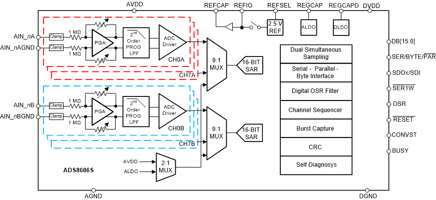
The ADS8686S is a 16-channel data acquisition (DAQ) system based on a dual simultaneous-sampling, 16-bit successive approximation register (SAR) analog-to-digital converter (ADC). The ADS8686S features a complete analog front-end for each channel with an input clamp, 1-MΩ input impedance, independently programmable gain amplifier (PGA), programmable low-pass filter, and an ADC input driver. The device also features a low-drift, precision reference with a buffer to drive the ADCs. A flexible digital interface supporting serial, parallel, and byte communication enables the device to be used with a variety of host controllers.
The ADS8686S can be configured to accept ±10-V, ±5-V, or ±2.5-V bipolar inputs with a 20% overrange option using a single 5-V supply. The high input impedance allows direct connection with sensors and transformers, thus eliminating the need for external driver circuits. The ADS8686S has a highly configurable channel sequencer to reduce the sequencing overhead on the backend controller or processor. The high performance and accuracy, along with zero-latency conversions offered by this device make the ADS8686S a great choice for multiple industrial applications.
| PART NUMBER | PACKAGE | BODY SIZE (NOM) |
|---|---|---|
| ADS8686S | LQFP (80) | 14.00 mm x 14.00 mm |
 Device Block Diagram