SBAS905C November 2019 – July 2020 ADS8686S
PRODUCTION DATA
- 1 Features
- 2 Applications
- 3 Description
- 4 Revision History
- 5 Pin Configuration and Functions
-
6 Specifications
- 6.1 Absolute Maximum Ratings
- 6.2 ESD Ratings
- 6.3 Recommended Operating Conditions
- 6.4 Thermal Information
- 6.5 Electrical Characteristics
- 6.6 Timing Requirements
- 6.7 Switching Characteristics
- 6.8 Timing Diagrams: Universal
- 6.9 Timing Diagrams: Parallel Data Read
- 6.10 Timing Diagrams: Serial Data Read
- 6.11 Typical Characteristics
-
7 Detailed Description
- 7.1 Overview
- 7.2 Functional Block Diagram
- 7.3 Feature Description
- 7.4
Device Functional Modes
- 7.4.1
Device Interface: Pin Description
- 7.4.1.1 REFSEL (Input)
- 7.4.1.2 RESET (Input)
- 7.4.1.3 SEQEN (Input)
- 7.4.1.4 HW_RANGESEL[1:0] (Input)
- 7.4.1.5 SER/BYTE/PAR (Input)
- 7.4.1.6 DB[3:0] (Input/Output)
- 7.4.1.7 DB4/SER1W (Input/Output)
- 7.4.1.8 DB5/CRCEN (Input/Output)
- 7.4.1.9 DB[7:6] (Input/Output)
- 7.4.1.10 DB8 (Input/Output)
- 7.4.1.11 DB9/BYTESEL (Input/Output)
- 7.4.1.12 DB10/SDI (Input/Output)
- 7.4.1.13 DB11/SDOB (Input/Output)
- 7.4.1.14 DB12/SDOA (Input/Output)
- 7.4.1.15 DB13/OS0 (Input/Output)
- 7.4.1.16 DB14/OS1 (Input/Output)
- 7.4.1.17 DB15/OS2 (Input/Output)
- 7.4.1.18 WR/BURST (Input)
- 7.4.1.19 SCLK/RD (Input)
- 7.4.1.20 CS (Input)
- 7.4.1.21 CHSEL[2:0] (Input)
- 7.4.1.22 BUSY (Output)
- 7.4.1.23 CONVST (Input)
- 7.4.2 Device Modes of Operation
- 7.4.1
Device Interface: Pin Description
- 7.5 Programming
- 7.6 Register Maps
- 8 Application and Implementation
- 9 Power Supply Recommendations
- 10Layout
- 11Device and Documentation Support
7.4.2.5.1 Hardware Mode Sequencer
In hardware mode, the sequencer has limited functionality. The sequencer always selects a particular channel pair (for example, AIN_nA and AIN_nB).
In hardware mode, the sequencer is controlled by the SEQEN pin and the CHSEL[2:0] pins. The logic level of the SEQEN pin is latched when RESET transitions from logic low to high after a full reset. Table 7-8 explains the sequencer setting based on the logic state of the SEQEN pin after a full reset. A full reset is required to exit sequencer mode and to setup an alternate configuration.
| SEQEN | INTERFACE MODE |
|---|---|
| 0 | Sequencer disabled |
| 1 | Sequencer enabled |
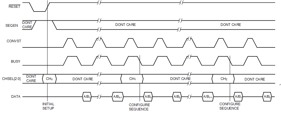
When the sequencer is enabled, the logic levels of the CHSEL[2:0] pins determine the number of channel pairs selected for the conversion in the sequence. The CHSEL[2:0] pins at the time when RESET is released determine the initial settings for the channels to convert in the first sequence. To reconfigure the sequence channels selected for a conversion thereafter, set the CHSEL[2:0] pins to the required setting for the duration of the BUSY pulse for the final conversion in the sequence. Table 7-9 explains the relationship between the CHSEL[2:0] pin to the channel pairs selected in the sequence. See Figure 7-16 for further timing sequence details.
| CHANNEL SELECTION INPUT PIN | ANALOG INPUT CHANNELS FOR SEQUENTIAL CONVERSION | |||
|---|---|---|---|---|
| CHSEL2 | CHSEL1 | CHSEL0 | ||
| 0 | 0 | 0 | AIN_0A, AIN_0B only | |
| 0 | 0 | 1 | AIN_0A, AIN_0B to AIN_1A, AIN_1B | |
| 0 | 1 | 0 | AIN_0A, AIN_0B to AIN_2A, AIN_2B | |
| 0 | 1 | 1 | AIN_0A, AIN_0B to AIN_3A, AIN_3B | |
| 1 | 0 | 0 | AIN_0A, AIN_0B to AIN_4A, AIN_4B | |
| 1 | 0 | 1 | AIN_0A, AIN_0B to AIN_5A, AIN_5B | |
| 1 | 1 | 0 | AIN_0A, AIN_0B to AIN_6A, AIN_6B | |
| 1 | 1 | 1 | AIN_0A, AIN_0B to AIN_7A, AIN_7B | |
 Figure 7-16 Hardware Mode Sequencer Configuration