SBAS905C November 2019 – July 2020 ADS8686S
PRODUCTION DATA
- 1 Features
- 2 Applications
- 3 Description
- 4 Revision History
- 5 Pin Configuration and Functions
-
6 Specifications
- 6.1 Absolute Maximum Ratings
- 6.2 ESD Ratings
- 6.3 Recommended Operating Conditions
- 6.4 Thermal Information
- 6.5 Electrical Characteristics
- 6.6 Timing Requirements
- 6.7 Switching Characteristics
- 6.8 Timing Diagrams: Universal
- 6.9 Timing Diagrams: Parallel Data Read
- 6.10 Timing Diagrams: Serial Data Read
- 6.11 Typical Characteristics
-
7 Detailed Description
- 7.1 Overview
- 7.2 Functional Block Diagram
- 7.3 Feature Description
- 7.4
Device Functional Modes
- 7.4.1
Device Interface: Pin Description
- 7.4.1.1 REFSEL (Input)
- 7.4.1.2 RESET (Input)
- 7.4.1.3 SEQEN (Input)
- 7.4.1.4 HW_RANGESEL[1:0] (Input)
- 7.4.1.5 SER/BYTE/PAR (Input)
- 7.4.1.6 DB[3:0] (Input/Output)
- 7.4.1.7 DB4/SER1W (Input/Output)
- 7.4.1.8 DB5/CRCEN (Input/Output)
- 7.4.1.9 DB[7:6] (Input/Output)
- 7.4.1.10 DB8 (Input/Output)
- 7.4.1.11 DB9/BYTESEL (Input/Output)
- 7.4.1.12 DB10/SDI (Input/Output)
- 7.4.1.13 DB11/SDOB (Input/Output)
- 7.4.1.14 DB12/SDOA (Input/Output)
- 7.4.1.15 DB13/OS0 (Input/Output)
- 7.4.1.16 DB14/OS1 (Input/Output)
- 7.4.1.17 DB15/OS2 (Input/Output)
- 7.4.1.18 WR/BURST (Input)
- 7.4.1.19 SCLK/RD (Input)
- 7.4.1.20 CS (Input)
- 7.4.1.21 CHSEL[2:0] (Input)
- 7.4.1.22 BUSY (Output)
- 7.4.1.23 CONVST (Input)
- 7.4.2 Device Modes of Operation
- 7.4.1
Device Interface: Pin Description
- 7.5 Programming
- 7.6 Register Maps
- 8 Application and Implementation
- 9 Power Supply Recommendations
- 10Layout
- 11Device and Documentation Support
7.4.2.5.2 Software Mode Sequencer
In software mode, the ADS8686S offers a 32-stack, fully configurable sequencer. The configuration register and sequencer stack registers can be programmed by using the parallel, byte, or serial interface.
Each stack register has two 4-bit fields to control each individual MUX. This structure allows any input from channel AIN_nA to be paired with any input from channel AIN_nB, or to any diagnostic channel. The sequencer depth is programmable from 1 to 32. The sequencer depth is determined by setting the SSRENx bit in the sequencer stack register corresponding to the last step. The channels to convert are selected by programming the ASELx and BSELx bits in each sequence stack register for the depth required.
The sequencer is activated by setting the SEQEN bit in the configuration register to 1.
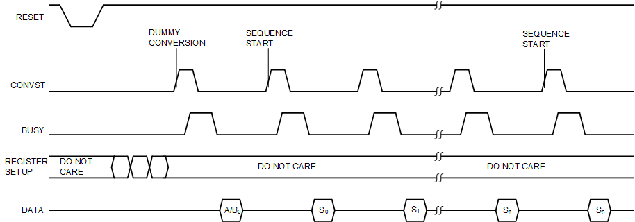
The recommended procedure to configure and enable the sequencer (see Figure 7-17 for additional information) is as follows:
- Program the analog input range for the required analog input channels.
- Program the sequencer stack registers (S0, S1,...Sn) to select the channels for the sequence.
- Set the SSRENx bit in the last required sequence step.
- Set the SEQEN bit in the configuration register.
- Provide a dummy CONVST pulse.
- Provide additional CONVST pulses and read the conversion results.
After all sequence steps are cycled through, the sequence automatically restarts from the first element in the sequencer stack with the next CONVST pulse.
Following a partial reset, the sequencer pointer is repositioned to the first layer of the stack, but the register programmed values remain unchanged.
 Figure 7-17 Software Mode Sequencer Configuration