SBASAS5 October   2025 AMC0100R

PRODUCTION DATA  

  1.   1
  2. Features
  3. Applications
  4. Description
  5. Pin Configuration and Functions
  6. Specifications
    1. 5.1 Absolute Maximum Ratings
    2. 5.2 ESD Ratings
    3. 5.3 Recommended Operating Conditions
    4. 5.4 Thermal Information (DEN Package)
    5. 5.5 Package Characteristics
    6. 5.6 Electrical Characteristics
    7. 5.7 Switching Characteristics
    8. 5.8 Timing Diagram
    9. 5.9 Typical Characteristics
  7. Detailed Description
    1. 6.1 Overview
    2. 6.2 Functional Block Diagram
    3. 6.3 Feature Description
      1. 6.3.1 Analog Input
      2. 6.3.2 Isolation Channel Signal Transmission
      3. 6.3.3 Analog Output
    4. 6.4 Device Functional Modes
  8. Application and Implementation
    1. 7.1 Application Information
    2. 7.2 Typical Application
      1. 7.2.1 Design Requirements
      2. 7.2.2 Detailed Design Procedure
        1. 7.2.2.1 Shunt Resistor Sizing
        2. 7.2.2.2 Input Filter Design
        3. 7.2.2.3 Designing the Bootstrap Supply
        4. 7.2.2.4 Connecting the REFIN Pin
      3. 7.2.3 Application Curves
    3. 7.3 Best Design Practices
    4. 7.4 Power Supply Recommendations
    5. 7.5 Layout
      1. 7.5.1 Layout Guidelines
      2. 7.5.2 Layout Example
  9. Device and Documentation Support
    1. 8.1 Documentation Support
      1. 8.1.1 Related Documentation
    2. 8.2 Receiving Notification of Documentation Updates
    3. 8.3 Support Resources
    4. 8.4 Trademarks
    5. 8.5 Electrostatic Discharge Caution
    6. 8.6 Glossary
  10. Revision History
  11. 10Mechanical, Packaging, and Orderable Information

Typical Characteristics

at VDD1 = 5V, VDD2 = 3.3V, VREFIN = 3.3V, VINP = –250mV to 250mV, VINN = 0V, and fIN = 10kHz (unless otherwise noted)

AMC0100R Output Voltage vs Input Voltage
 
Figure 5-2 Output Voltage vs Input Voltage
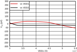
AMC0100R Input Offset Voltage vs Supply
                                    Voltage
 
Figure 5-4 Input Offset Voltage vs Supply Voltage
AMC0100R Input Offset Voltage vs VREFIN
VDD2 = 3.3V
Figure 5-6 Input Offset Voltage vs VREFIN
AMC0100R Gain Error vs
                                    VREFIN
VDD2 = 3.3V
Figure 5-8 Gain Error vs VREFIN
AMC0100R Gain Error vs Supply Voltage
 
Figure 5-10 Gain Error vs Supply Voltage
AMC0100R Common-Mode Rejection Ratio vs Supply
                                    Voltage
 
Figure 5-12 Common-Mode Rejection Ratio vs Supply Voltage
AMC0100R Common-Mode Rejection Ratio vs
                                    Temperature
 
Figure 5-14 Common-Mode Rejection Ratio vs Temperature
AMC0100R Input Current vs Temperature
 
Figure 5-16 Input Current vs Temperature
AMC0100R Output Phase vs Input Frequency
 
Figure 5-18 Output Phase vs Input Frequency
AMC0100R Nonlinearity vs Supply Voltage
 
Figure 5-20 Nonlinearity vs Supply Voltage
AMC0100R Total Harmonic Distortion vs Supply
                                    Voltage
 
Figure 5-22 Total Harmonic Distortion vs Supply Voltage
AMC0100R Input-Referred Noise Density vs
                                    Frequency
 
Figure 5-24 Input-Referred Noise Density vs Frequency
AMC0100R Signal-to-Noise Ratio vs Supply
                                    Voltage
 
Figure 5-26 Signal-to-Noise Ratio vs Supply Voltage
AMC0100R Power-Supply Rejection Ratio vs Ripple
                                    Frequency
 
Figure 5-28 Power-Supply Rejection Ratio vs Ripple Frequency
AMC0100R Power-Supply Rejection Ratio vs
                                    Temperature
 
Figure 5-30 Power-Supply Rejection Ratio vs Temperature
AMC0100R Output Bandwidth vs Temperature
 
Figure 5-32 Output Bandwidth vs Temperature
AMC0100R Supply Current vs Temperature
 
Figure 5-34 Supply Current vs Temperature
AMC0100R Output Rise and Fall Time vs
                                    Temperature
 
Figure 5-36 Output Rise and Fall Time vs Temperature
AMC0100R VIN to VOUT Signal
                                    Delay vs Temperature
 
Figure 5-38 VIN to VOUT Signal Delay vs Temperature
AMC0100R Unadjusted Error vs Input Voltage
Total uncalibrated output error is defined as:((VOUT_Measured – VOUT_Expected) / VREFIN) x 100 , where VOUT_Expected = VIN / VClipping x VREFIN / 2 + VREFIN / 2, VREFIN = 3.3V and VClipping = 0.32V
Figure 5-3 Unadjusted Error vs Input Voltage
AMC0100R Input Offset Voltage vs Temperature
 
Figure 5-5 Input Offset Voltage vs Temperature
AMC0100R Input Offset Voltage vs VREFIN
VDD2 = 5.5V
Figure 5-7 Input Offset Voltage vs VREFIN
AMC0100R Gain Error vs
                                    VREFIN
VDD2 = 5.5V
Figure 5-9 Gain Error vs VREFIN
AMC0100R Gain Error vs Temperature
 
Figure 5-11 Gain Error vs Temperature
AMC0100R Common-Mode Rejection Ratio vs Input
                                    Frequency
 
Figure 5-13 Common-Mode Rejection Ratio vs Input Frequency
AMC0100R Input Current vs Input Voltage
 
Figure 5-15 Input Current vs Input Voltage
AMC0100R Normalized Gain vs Input Frequency
 
Figure 5-17 Normalized Gain vs Input Frequency
AMC0100R Nonlinearity vs Input Voltage


Figure 5-19 Nonlinearity vs Input Voltage
AMC0100R Nonlinearity vs Temperature
 
Figure 5-21 Nonlinearity vs Temperature
AMC0100R Total Harmonic Distortion vs
                                    Temperature
 
Figure 5-23 Total Harmonic Distortion vs Temperature
AMC0100R Signal-to-Noise Ratio vs Input
                                    Voltage
 
Figure 5-25 Signal-to-Noise Ratio vs Input Voltage
AMC0100R Signal-to-Noise Ratio vs
                                    Temperature
 
Figure 5-27 Signal-to-Noise Ratio vs Temperature
AMC0100R Power-Supply Rejection Ratio vs Supply
                                    Voltage
 
Figure 5-29 Power-Supply Rejection Ratio vs Supply Voltage
AMC0100R Output Bandwidth vs Low-Side Supply
                                    Voltage
 
Figure 5-31 Output Bandwidth vs Low-Side Supply Voltage
AMC0100R Supply Current vs Supply Voltage
 
Figure 5-33 Supply Current vs Supply Voltage
AMC0100R Output Rise and Fall Time vs Low-Side
                                    Supply
 
Figure 5-35 Output Rise and Fall Time vs Low-Side Supply
AMC0100R VIN to VOUT Signal
                                    Delay vs Low-Side Supply Voltage
 
Figure 5-37 VIN to VOUT Signal Delay vs Low-Side Supply Voltage