Typical values at TA = +25°C, ADC
Sampling Rate = 2949.12GHz. Default conditions: output sample rate =
491.52MSPS (decimate by 6), PLL clock mode with fREF =
491.52MHz, AIN = –3dBFS, DSA setting = 4dB.

| With matching, normalized to power at 4.9GHz for each DSA setting |

| With 4.9GHz matching, normalized to phase at
25°C |
|
|

| With 4.9GHz matching |
| Differential Amplitude Error = PIN (DSA
Setting – 1) – PIN (DSA Setting) + 1 |

| With 4.9GHz matching |
| Integrated Amplitude Error = PIN (DSA
Setting) – PIN (DSA Setting = 0) + (DSA
Setting) |

| With 4.9GHz matching |
| Differential Phase Error = PhaseIN (DSA
Setting – 1) – PhaseIN (DSA Setting) |

| With 4.9GHz matching |
| Integrated Phase Error = Phase (DSA Setting) – Phase
(DSA Setting = 0) |

| With 4.9GHz matching, 12.5MHz offset from
tone |
|

| With 4.9GHz matching, 12.5MHz offset from
tone |
|

| With 4.9GHz matching, tone spacing = 20MHz,
DSA = 4dB |
|

| With 4.9GHz matching, measured after HD2 trim,
DDC bypass mode (TI only mode for
characterization) |

| With 4.9GHz matching, measured after HD2 trim,
DDC bypass mode (TI only mode for
characterization) |

| With 4.9GHz matching, DDC bypass mode (TI only
mode for characterization) |

| With 4.9GHz matching, DDC bypass mode (TI only
mode for characterization) |
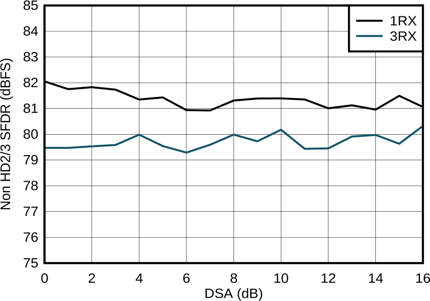 Figure 4-199 RX Non-HD2/3 vs DSA
Setting at 4.9GHz
Figure 4-199 RX Non-HD2/3 vs DSA
Setting at 4.9GHz
| With 4.9GHz matching, 12.5MHz offset, all
supplies at MIN, TYP, or MAX recommended operating
voltages |
|

| With 4.9GHz matching, normalized to fullscale
at 25°C for each channel |

| With 4.9GHz matching |
| Differential Amplitude Error = PIN (DSA
Setting – 1) – PIN (DSA Setting) + 1 |

| With 4.9GHz matching |
| Integrated Amplitude Error = PIN (DSA
Setting) – PIN (DSA Setting = 0) + (DSA
Setting) |

| With 4.9GHz matching |
| Differential Phase Error = PhaseIN (DSA
Setting – 1) – PhaseIN (DSA Setting) |

| With 4.9GHz matching |
| Integrated Phase Error = Phase (DSA Setting) – Phase
(DSA Setting = 0) |

| With 4.9GHz matching, fIN =
4910MHz, AIN= –3dBFS |
|
|

| With 4.9GHz matching, DSA Setting = 12dB,
12.5MHz offset from tone |

| With 4.9GHz matching, each tone –7dBFS, tone
spacing = 20MHz |

| With 4.9GHz matching, tone spacing = 20MHz,
DSA = 12dB |

| With 4.9GHz matching, measured after HD2 trim,
DDC bypass mode (TI only mode for
characterization) |

| With 4.9GHz matching, DDC bypass mode (TI only
mode for characterization) |

| With 4.9GHz matching, DDC bypass mode (TI only
mode for characterization) |

| With 4.9GHz matching, decimate by 3 |

| With 4.9GHz matching, –7dBFS each tone, 20MHz
tone spacing, all supplies at MIN, TYP, or MAX
recommended operating voltages |