SBAU321B November   2018  – June 2021 ADS7142 , ADS7142-Q1


  1.   Trademarks
  2. 1Introduction
  3. 2BOOSTXL-ADS7142-Q1 EVM Overview
    1. 2.1 Connectors for Single-Ended Analog Input
    2. 2.2 Digital Interface
    3. 2.3 ADS7142-Q1 Digital I/O Interface
    4. 2.4 Power Supplies
  4. 3BOOSTXL-ADS7142-Q1 EVM Initial Setup
    1. 3.1 Running ADS7142-Q1 GUI Online and TI Cloud Agent Application Installation
    2. 3.2 Hardware Setup Instructions
    3. 3.3 ADS7142-Q1 GUI Description
      1. 3.3.1 Description
      2. 3.3.2 REGMAP
      3. 3.3.3 Functional Mode
      4. 3.3.4 General Instructions
  5. 4ADS7142-Q1 GUI Functional Modes
    1. 4.1 Autonomous Mode
      1. 4.1.1 Start Burst Mode
      2. 4.1.2 Stop Burst Mode
      3. 4.1.3 Pre Alert Mode
      4. 4.1.4 Post Alert Mode
    2. 4.2 High Precision Mode
    3. 4.3 Manual Mode
      1. 4.3.1 Default Mode
      2. 4.3.2 Auto Mode
    4. 4.4 Temperature Monitoring Using BOOSTXL-ADS7142-Q1
    5. 4.5 Input Signal Conditioning Block on the BOOSTXL-ADS7142-Q1
  6. 5Bill of Materials, Printed-Circuit Board Layout, and Schematics
    1. 5.1 Bill of Materials
    2. 5.2 PCB Layout
    3. 5.3 Schematics
  7. 6Revision History

Hardware Setup Instructions

The following are the instructions to set up the BOOSTXL-ADS7142-Q1 for evaluation:

  1. Stack the BOOSTXL-ADS7142-Q1 on the PAMB. Make sure the 20-pin connector (J1 and J3) on BOOSTXL-ADS7142-Q1 is mapped against the left PAMB connector and the connector (J4 and J2) on BOOSTXL-ADS7142-Q1 is mapped against the right PAMB connector. Pin 1 of BOOSTXL-ADS7142-Q1 must align with pin 1 of left PAMB connector (3V3)
  2. Connect the micro USB from data port o PAMB to available USB port on PC.
  3. Figure 3-2 shows the assembled BOOSTXL-ADS7142-Q1 and PAMB configuration.
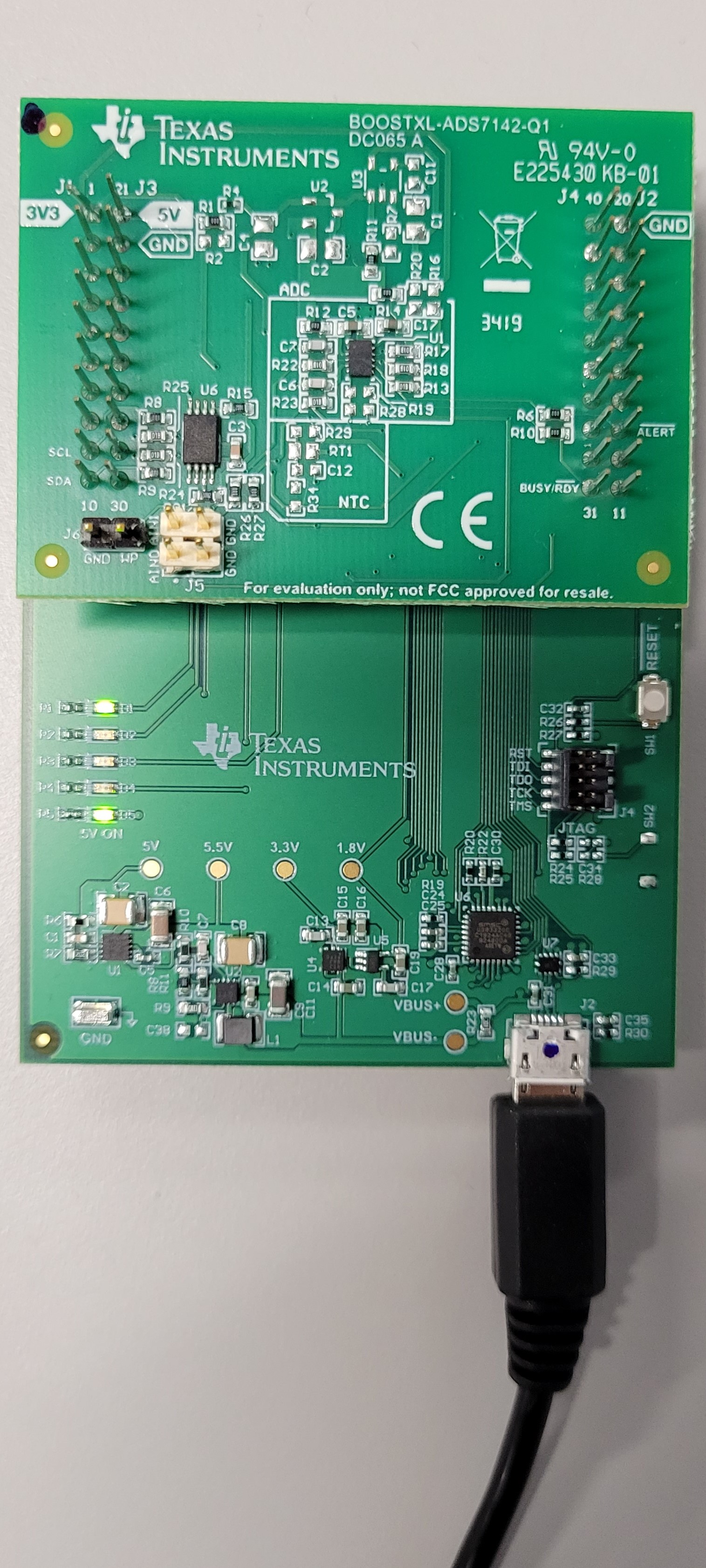
    GUID-CC723C8A-BE65-405A-875A-0320D87DCDE2-low.jpg Figure 3-2 BOOSTXL-ADS7142-Q1 Stacked on PAMBoard