SBAU352 June 2020 ADS131B04-Q1
2.2 ADC External Clock (CLKIN) Options
The ADS131B04-Q1 requires a continuous, free-running external master clock at the CLKIN pin for normal operation. The onboard complementary metal oxide semiconductor (CMOS) crystal oscillator (Y1) provides the nominal 8.192-MHz clock frequency used in the high-resolution (HR) mode of the device. Two D flip-flops (U3) divide the Y1 clock output to produce clock frequencies of 4.096 MHz and 2.048 MHz to support the low-power (LP) mode and very-low-power (VLP) mode, respectively.
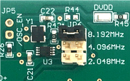
Install a jumper in the appropriate position on the JP6 header shown in Figure 4 to provide selectable clock frequency options. An external clock frequency can also be provided to any even-numbered pin on JP6 when the jumper is uninstalled. TI also recommends powering down Y1 by installing JP5 when providing an external clock. When using an external clock, ground must be shared between the external clock source and the EVM ground. The external clock must adhere to the frequency and amplitude limits outlined in the ADS131B04-Q1 data sheet. Table 4 lists the JP6 jumper settings for the clock input selections.
In addition to jumper settings, each of the power modes requires configuration register settings outlined in Section 6.1.
 Figure 4. CLKIN External Clock (PCB)
 Table 4. CLKIN External Clock Options
| J13 Jumper Setting | Clock Frequency | Description |
|---|---|---|
| [1-2] | 8.192 MHz | Nominal clock for high-resolution mode (default) |
| [3-4] | 4.096 MHz | Nominal clock for low-power mode |
| [5-6] | 2.048 MHz | Nominal clock for very-low-power mode |