SBOU227A September 2019 – November 2023 ALM2402F-Q1
3 Jumper Settings
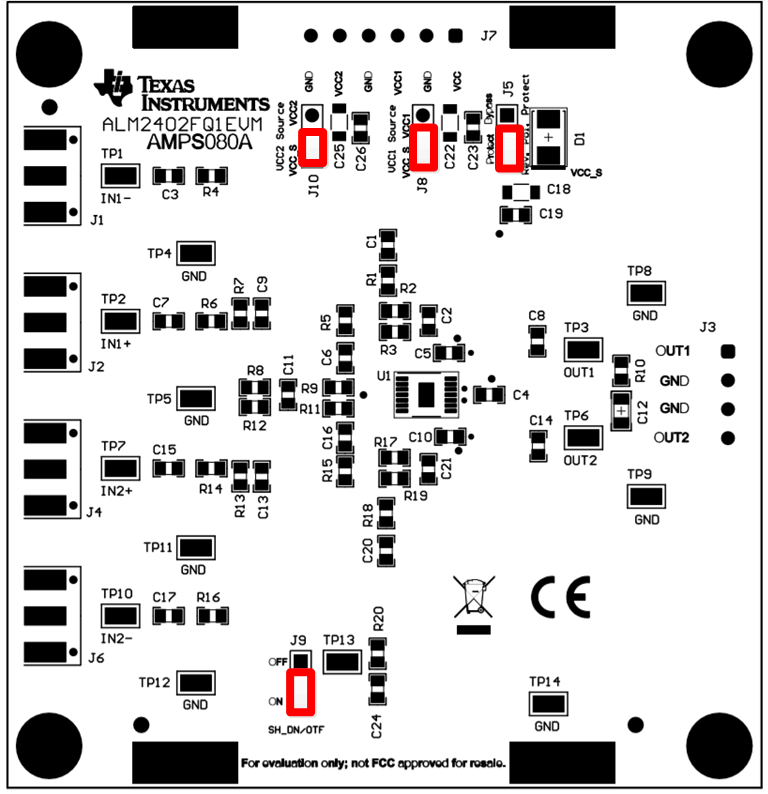
Figure 3-1 details the default jumper settings of the ALM2402FQ1EVM. Figure 3-1 explains the configuration for these jumpers.
 Figure 3-1 ALM2402FQ1
Evaluation Module Default Jumper Settings
Figure 3-1 ALM2402FQ1
Evaluation Module Default Jumper Settings| Jumper | Function | Default Position | Description |
|---|---|---|---|
| J5 | VCC_S reverse polarity protection | Shunt 2-3 | Shunt 2-3: Schottky diode blocks
VCC_S supply reverse current Shunt 1-2 bypasses VCC_S Schottky diode protection |
| J8 | VCC1 source | Shunt 1-2 | Shunt 1-2 selects VCC_S for op amp1
output supply Shunt 2-3 selects VCC_1 for op amp 1 output supply |
| J10 | VCC2 source | Shunt 1-2 | Shunt 1-2 selects VCC_S for op amp2
output supply Shunt 2-3 selects VCC_2 for op amp 2 output supply |
| J9 | SH_DN / OTF | Shunt 2-3 | Overtemperature flag or shutdown:
Shunt 2-3 turns on amplifiers; pin works as overtemperature flag Shunt 1-2 shuts down amplifiers |
The SH_DN/OTF's pull-up voltage larger than 7 V can permanently damage the device, see the Absolute Maximum Ratings of ALM2402F-Q1’s data sheet.
If the supply voltage VCC_S is greater than 5 V, then the pull-up resistor R20 must be removed and the SH_DN/OTF pin must be driven from a separate voltage source, or a 4.7 V Zener needs to be added to the SH_DN/OTF pin as shown in Figure 2-1 and Figure 7-1.
Note: The 4.7 V Zener clamp has not implemented into the existing AMPS080_A EVM .