SCLA053A August 2022 – September 2022 SN74HCS08 , SN74HCS125 , SN74HCS14 , SN74HCS32 , SN74LVC08A , SN74LVC125A , SN74LVC14A , SN74LVC2G32
1
Introduction
To get the most out of your board space and the wide selection of packages available from Texas Instruments, consider using a dual footprint. The term dual footprint here refers to overlaying two PCB landing pads for two different package configurations. In supply constrained environments, this is a great method to mitigate supply issues for new designs or board spins.
There are many different package types and configurations available that enable overlaying their landing pads while occupying an optimized board area. Clearance rules must always be observed and are dependent on voltage and power requirements. TI's logic devices work at low voltages, so generally clearances are very small and allow for this type of operation. This application brief will cover examples for dual footprints using industry standard packages both leaded and leadless. All examples will have a minimum of 5 mil clearance between any traces.
Leaded to Leadless Packages
Combined footprints from leaded to leadless packages are ideal as long as they have the same pin count and similar pin orientation. TI's latest QFN packages are some of the industries smallest packages, they will easily fit inside the land pattern of numerous larger leaded packages. This allows for easy routing to each corresponding pin without any vias. An ample amount of TI's most popular devices are offered in both leaded and leadless packages, allowing for effortless drop-in replacements.
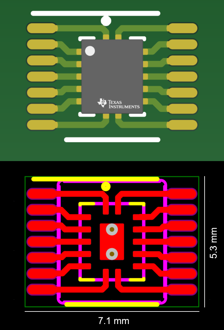
 Figure 1-1 PW + BQA Dual Footprint
Figure 1-1 shows a dual footprint for a TSSOP (PW) 14 pin package and a WQFN (BQA) 14 pin package.
Package Sizes:
- 14-Pin PW: 37.63 mm2
- 14-Pin BQA: 11.16 mm2
Total Board Space Used:
- PW + BQA: 37.63 mm2
TI's latest logic family, HCS, offers the most popular functions in the PW, DYY and BQA packages.
| Part Number | Vcc Range | Type | Features |
|---|---|---|---|
| SN74HCS08 | 2 V to 6 V | AND Gate | Schmitt-trigger inputs 4 Channels |
| SN74HCS32 | 2 V to 6 V | OR Gate | Schmitt-trigger inputs 4 Channels |
| SN74HCS14 | 2 V to 6 V | Inverter | Schmitt-trigger inputs 6 Channels |
| SN74HCS125 | 2 V to 6 V | Buffer | Schmitt-trigger inputs 3-State outputs 4 Channels |
Leaded to Leaded Packages
Leaded packages are easily leveraged for dual footprints as long as they have the same pin count and similar lead pitches. Board traces are routed between the corresponding pins of each package. Vias can be used to connect certain leads between packages to meet PCB trace clearance rules.
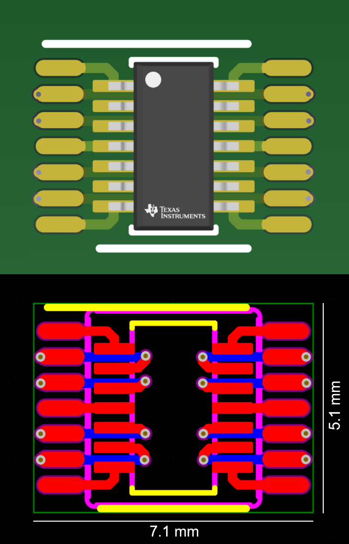
When combining packages with similar pin configurations the smaller package footprint can sometimes be used within the land pattern area of the larger package. Figure 1-2 shows an example of this for an SOT (DYY) and a TSSOP (PW) package.
 Figure 1-2 PW + DYY Dual Footprint
Package Sizes:
- 14-Pin PW: 37.63 mm2
- 14-Pin DYY: 20.4 mm2
Total Board Space Used:
- PW + DYY: 37.63 mm2
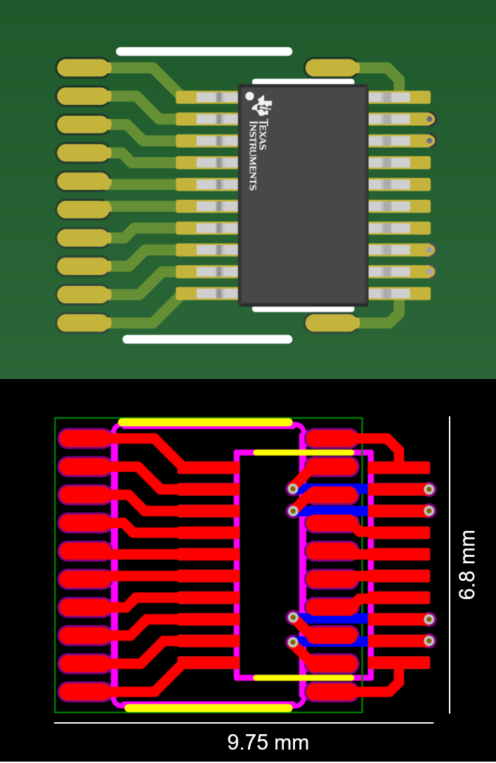
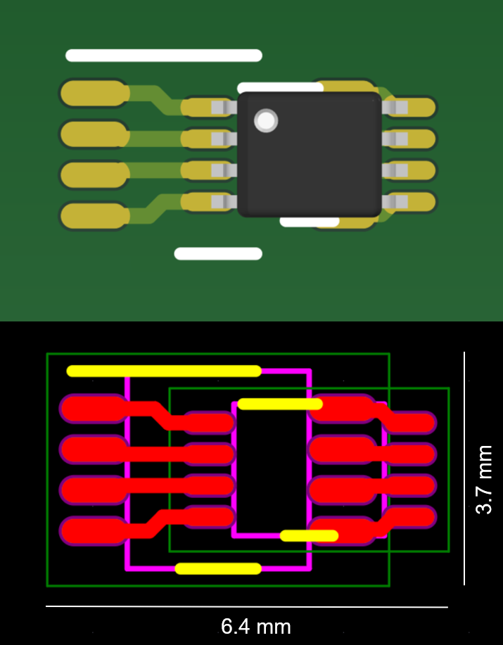
Package combinations where the smaller package does not fit inside the larger package can still be used in dual footprints by overlapping the packages as shown in Figure 1-3 and Figure 1-4.
 Figure 1-3 PW + DGS Dual Footprint
Figure 1-3 shows a dual footprint for a TSSOP (PW) 20 pin package and a VSSOP (DGS) 20 pin package.
Package Sizes:
- 20-Pin PW: 48.28 mm2
- 20-Pin DGS: 34.49 mm2
Total Board Space Used:
- PW + DGS: 59.84 mm2
 Figure 1-4 DCU + DCT Dual Footprint
Figure 1-4 shows a dual footprint for a VSSOP (DCU) 8 pin package and a SSOP (DCT) 8 pin package.
Package Sizes:
- 8-Pin DCU: 11.57 mm2
- 8-Pin DCT: 20.17 mm2
Total Board Space Used:
- DCU + DCT: 23.68 mm2
TI's most popular logic family, LVC, offers the most popular functions in the PW, DGS, DCU and DCT packages.
| Part Number | Vcc Range | Type | Features |
|---|---|---|---|
| SN74LVC08A | 1.65 V to 3.6 V | AND Gate | High drive strength 4 Channels |
| SN74LVC2G32 | 1.65 V to 5.5 V | OR Gate | High drive strength 2 Channels |
| SN74LVC14A | 1.65 V to 3.6 V | Inverter | High drive strength 6 Channels |
| SN74LVC125A | 1.65 V to 3.6 V | Buffer | High drive strength 3-State outputs 1 Channel |
Design Considerations
When designing dual footprints with logic devices the main concern is to maintain at least a 5 mil clearance between the pads of both devices. This will prevent the solder mask from being applied inadequately in the manufacturing process. If solder mask is not applied properly, the device can shift during the reflow process potentially causing floating pins or short circuits. An additional concern, mainly for noisy environments, is that one device will have a longer trace from the supply pin to the bypass capacitor making it slightly more susceptible to noise.
Conclusion
Dual footprints are an excellent method to future-proof your designs, providing multi-sourced sockets to prevent supply constraints while maintaining similar size to a typical single footprint option. The combined footprints shown are just a few examples. Many more package combinations are possible using the huge portfolio available from TI.