SCPA063 March 2023 PCA9306
2.3 Double Check SDA and SCL Between the Controller and Target
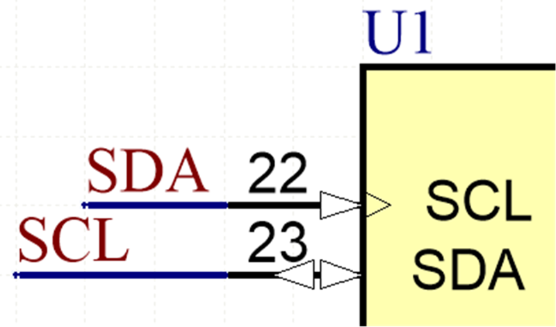
If NACKs are being received from an I2C device the design is communicating with, check to make sure that the SDA and SCL lines are properly connected between the I2C controller and target. Sometimes users accidentally swap the SDA and SCL connections between a controller and target device. If this happens, the target device always sends NACKs back to the controller, even if the correct bits are being transmitted. To prevent this from happening, always verify that the SDA and SCL connections between the controller and the target are correct. Figure 2-4 shows an example where the SDA and SCL nets on the schematic are swapped with the schematic pinout SDA and SCL resulting in the I2C target device always NACKing the address.
 Figure 2-4 Example of SDA and SCL Nets Swapped in Schematic