SDAA444 October 2026 UCC23711
- 1
- Abstract
- Trademarks
- 1Introduction
- 2Opto-Input Isolated Protection Gate Driver for SiC and IGBT
- 3Three Phase IGBT Inverter Design Guidelines for UCC23711
-
4System Test
Results
- 4.1 Three-Phase IGBT Inverter under Test
- 4.2 UCC23711 Input Current Thresholds and Hysteresis
- 4.3 UCC23711 Propagation Delay
- 4.4 Phase U Turn-On and Turn-Off Slew Rates
- 4.5 UCC23711 Miller Clamp and Unipolar 15V Supply
- 4.6 UCC23711 DESAT Response and Soft Shut Down
- 4.7 Increasing the DESAT Charge Current
- 4.8 UCC23711 VDD UVLO Thresholds and Gate Drive Output
- 4.9 UCC23711 Gate Drive Power Consumption
- 5Summary
- 6References
3.3 UCC23711 Gate Drive Turn-on and Turn-off Peak Current
The gate drive output resistors R12, R13 and the Schottky diode D6, placed in parallel to R13, as shown in the following figure. This allows a configurable turn-on and turn-off peak current. With the default configuration R12=R13=5.1kΩ and D6 populated the UCC23711 source and sink peak currents can be estimated for a bipolar supply bipolar +15V and -8V supply with VDD-VEE=23V:
where RGint=0 is the selected IGBT's internal gate resistance and ROUTH =0.7Ω the UCC23711 output pull-up resistance for sorcing current.
where VF(D6) =0.3V, RGINT,IGBT=0 and ROUTL =0.7Ω the UCC23711 output pull-down resistance for sinking current.
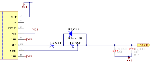 Figure 3-3 UCC23711 Gate Drive Circuit
The estimated peak current is also influenced by PCB layout and load capacitance. Parasitic inductance in the gate-driver loop can slow down the peak gate-drive current and introduce overshoot and undershoot. Therefore, the gate-driver current loop to the IGBT should be minimized.
The UCC23711 gate driver output stage implements an active pulldown feature to ensure the gate driver output pin is clamped to VEE when VDD is open. An optional 10k pull-down resistor R15 is placed close to the IGBT gate and emitter to discharge stray charges, for example when the connection between the gate driver and the IGBT fails, or when the gate drive supply powers up. Since the UCC23711 offers an active pull-down feature when VDD is off, R15 was not populated for the tests.
An option to place a capacitor C4 close to the IGBT gate and emitter has been provided to sink the additional charge originating from the Miller capacitance during the turn-on of top IGBT. Due to the additional capacitance, the effective input capacitance of the IGBT is C4||CGE, the gate charge required to reach the threshold voltage will be increased and the turn-on and off-times are slower. Since the UCC23711 offers an active Miller clamp, C4 is not populated.