SFFSAJ9A June 2025 – September 2025 UCC27289
4.1 SOIC Package
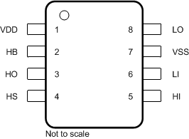
Figure 4-1 shows the UCC27289 pin diagram for the SOIC package. For a detailed description of the device pins please refer to the Pin Configuration and Functions section in the UCC27289 data sheet.
 Figure 4-1 Pin Diagram (SOIC Package)
Table 4-2 Pin FMA for Device Pins Short-Circuited to Ground
| Pin Name | Pin No. | Description of Potential Failure Effects | Failure Effect Class |
|---|---|---|---|
| VDD | 1 | LO remains low. HO remains low. | B |
| HB | 2 | Device can be damaged with unknown LO or HO state. | A |
| HO | 3 | Device can be damaged with unknown LO or HO state. | A |
| HS | 4 | Device can be damaged with unknown LO or HO state. | A |
| HI | 5 | HO is in a low state. | B |
| LI | 6 | LO is in a low state. | B |
| VSS | 7 | N/A | D |
| LO | 8 | Device can be damaged with unknown LO or HO state. | A |
Table 4-3 Pin FMA for Device Pins Open-Circuited
| Pin Name | Pin No. | Description of Potential Failure Effects | Failure Effect Class |
|---|---|---|---|
| VDD | 1 | LO remains low. HO remains low. | B |
| HB | 2 | HO is pulled to HS potential. | B |
| HO | 3 | HO terminal is not connected to the system. | D |
| HS | 4 | HO is pulled to HB potential. | B |
| HI | 5 | HO is in a low state. | B |
| LI | 6 | LO is in a low state. | B |
| VSS | 7 | HO is in a low state. LO is pulled to VDD. | B |
| LO | 8 | LO terminal is not connected to the system. | D |
Table 4-4 Pin FMA for Device Pins Short-Circuited to Adjacent Pin
| Pin Name | Pin No. | Shorted to (Pin Number +1) | Description of Potential Failure Effects | Failure Effect Class |
|---|---|---|---|---|
| VDD | 1 | HB | Device can be damaged. LO or HO can be damaged with unknown state. | A |
| HB | 2 | HO | Device can be damaged with unknown HO state. | A |
| HO | 3 | HS | Device can be damaged with unknown LO or HO state. | A |
| HS | 4 | N/A | N/A | N/A |
| HI | 5 | LI | HO or LO is in a low state. | B |
| LI | 6 | VSS | LO is in a low state. | B |
| VSS | 7 | LO | Device can be damaged with unknown LO or HO state. | A |
| LO | 8 | N/A | N/A | N/A |
Table 4-5 Pin FMA for Device Pins Short-Circuited to Supply
| Pin Name | Pin No. | Description of Potential Failure Effects | Failure Effect Class |
|---|---|---|---|
| VDD | 1 | No effect. | D |
| HB | 2 | Device can be damaged with unknown LO or HO state. | A |
| HO | 3 | Device can be damaged with unknown LO or HO state. | A |
| HS | 4 | Device can be damaged with unknown LO or HO state. | A |
| HI | 5 | Short to 5V (for example, power supply of the microcontroller). LO or HO follows the HI,LI truth table. | B |
| LI | 6 | Short to 5V (for example, power supply of the microcontroller). LO or HO follows the HI,LI truth table. | B |
| VSS | 7 | HO is in a low state. LO is pulled to VDD. | B |
| LO | 8 | Device can be damaged with unknown LO or HO state. | A |