SLAA476B February 2011 – July 2019 BQ2040 , BQ2040 , BQ2060A , BQ2060A , BQ2063 , BQ2063 , BQ2083-V1P3 , BQ2083-V1P3 , BQ2084-V143 , BQ2084-V143 , BQ2084-V150 , BQ2084-V150 , BQ2085-V1P3 , BQ2085-V1P3 , BQ20Z40-R1 , BQ20Z40-R1 , BQ20Z70-V160 , BQ20Z70-V160 , BQ20Z80A-V110 , BQ20Z80A-V110 , BQ28400 , BQ28400 , BQ78PL114 , BQ78PL114 , BQ78PL116 , BQ78PL116 , LM5145 , LM5145 , MSP430F5500 , MSP430F5500 , MSP430F5501 , MSP430F5501 , MSP430F5502 , MSP430F5502 , MSP430F5503 , MSP430F5503 , MSP430F5504 , MSP430F5504 , MSP430F5505 , MSP430F5505 , MSP430F5506 , MSP430F5506 , MSP430F5507 , MSP430F5507 , MSP430F5508 , MSP430F5508 , MSP430F5509 , MSP430F5509 , MSP430F5510 , MSP430F5510 , TPS40057 , TPS40057 , TPS40170 , TPS40170
-
Wide-Vin Battery Charger Using SMBus Communication Interface Between MSP430™ MCUs and bq Fuel Gauges
- Trademarks
- 1 Introduction
- 2 Hardware
- 3
Software
- 3.1 SMBus Protocol Description
- 3.2 Software File Structure
- 3.3
API Calls Description
- 3.3.1 UCS_Init ( )
- 3.3.2 Timer_Init ( )
- 3.3.3 PWM_Init ( )
- 3.3.4 ADC_Init ( )
- 3.3.5 Fan_Init ( )
- 3.3.6 LED_Init ( )
- 3.3.7 SMBus_Initialize ( )
- 3.3.8 LED_Control ( )
- 3.3.9 Fan_Control ( )
- 3.3.10 VI_ADC_Read ( )
- 3.3.11 SMBus_Select ( )
- 3.3.12 Calibrate_Battery ( )
- 3.3.13 Delay_Timer ( )
- 3.3.14 PWM_Control ( )
- 3.3.15 Smbus_Access ( )
- 3.3.16 Smbus_Access_PEC ( )
- 3.3.17 crc8MakeBitwise ( )
- 3.4 Sample Application Description
- 4 SBS Supported Commands Using SMBus Protocol
- 5 Detailed Sample Application Flow Chart
- 6 Battery Status Register Description
- 7 MSP430F5510 Daughterboard Schematics
- 8 Setting Up the MSP430F5510 Daughterboard Hardware
- 9 Battery Calibration Circuit Setup
- 10 Battery Voltage and PWM Conversions
- 11 Battery Current and PWM Conversions
- 12 Power Stage Board Schematics (Generation 1: 40-V Input)
- 13 Bode Plot Measurement for Feedback Loop Stability Analysis
- 14 Power Stage Board Schematics (Generation 2: 60-V Input)
- 15 Setting Up the Power Stage Board Hardware
- 16 References
- Revision History
2.3.2 Input Protection Features
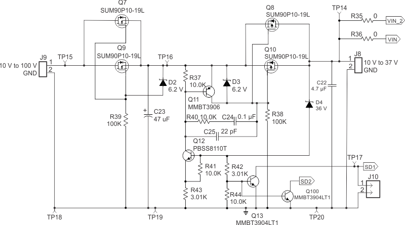
This reference design includes protection circuitry for both overvoltage (up to 100 V) as well as reverse voltage (positive and negative leads swapped). This portion of the circuitry is shown in Figure 5.
 Figure 5. Overvoltage and Reverse Polarity Protection Circuitry
 - Reverse voltage protection – FETs Q7 and Q9 along with D2 provide reverse voltage protection in case the input voltage is connected backwards. This does not allow a negative voltage to be applied to the system.
- Input overvoltage protection – FETs Q8 and Q10 provide an overvoltage protection circuit. The zener diode D4 sets the voltage that the circuit starts to clamp. Once the zener voltage is exceeded, the gate-to-source voltage of the FETs starts to drop. This causes the FETs to operate in the linear region. At the same time, the battery charging circuits are turned off with signals SD1 and SD2.